SLVSCI4B February 2014 – September 2014 TPS22961
PRODUCTION DATA.
- 1 Features
- 2 Applications
- 3 Description
- 4 Simplified Schematic
- 5 Revision History
- 6 Terminal Configuration and Functions
- 7 Specifications
- 8 Detailed Description
- 9 Applications and Implementation
- 10Power Supply Recommendations
- 11Layout
- 12Device and Documentation Support
- 13Mechanical, Packaging, and Orderable Information
Package Options
Refer to the PDF data sheet for device specific package drawings
Mechanical Data (Package|Pins)
- DNY|8
Thermal pad, mechanical data (Package|Pins)
Orderable Information
6 Terminal Configuration and Functions
DNY PACKAGE
8 TERMINAL
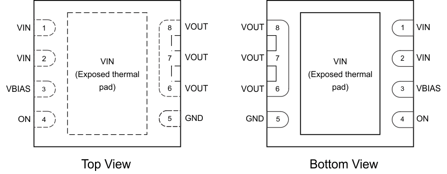
Pin Functions
| PIN | I/O | DESCRIPTION | |
|---|---|---|---|
| NAME | NO. | ||
| VIN | 1, 2 | I | Switch input. Place ceramic bypass capacitor(s) between this terminal and GND. See Detailed Description section for more information. |
| VIN | Exposed thermal Pad | I | Switch input. Place ceramic bypass capacitor(s) between this terminal and GND. See Detailed Description section for more information. |
| VBIAS | 3 | I | Bias voltage. Power supply to the device. |
| ON | 4 | I | Active high switch control input. Do not leave floating. |
| GND | 5 | – | Ground. |
| VOUT | 6, 7, 8 | O | Switch output. Place ceramic bypass capacitor(s) between this terminal and GND. See Detailed Description section for more information. |