SLVSBS6A June 2013 – January 2015 TPS22963C , TPS22964C
PRODUCTION DATA.
- 1 Features
- 2 Applications
- 3 Description
- 4 Simplified Schematic
- 5 Revision History
- 6 Device Comparison Table
- 7 Pin Configuration and Functions
- 8 Specifications
- 9 Parametric Measurement Information
- 10Detailed Description
- 11Application and Implementation
- 12Power Supply Recommendations
- 13Layout
- 14Device and Documentation Support
- 15Mechanical, Packaging, and Orderable Information
Package Options
Mechanical Data (Package|Pins)
- YZP|6
Thermal pad, mechanical data (Package|Pins)
Orderable Information
8 Specifications
8.1 Absolute Maximum Ratings
over operating free-air temperature range (unless otherwise noted)| MIN | MAX | UNIT | |||
|---|---|---|---|---|---|
| VIN | Input voltage range | –0.3 | 6 | V | |
| VOUT | Output voltage range | –0.3 | 6 | V | |
| VON | ON pin voltage range | –0.3 | 6 | V | |
| IMAX | Maximum continuous switch current | 3 | A | ||
| IPLS | Maximum pulsed switch current, 100 µs pulse, 2% duty cycle, TA = –40°C to 85°C | 4 | A | ||
| TA | Operating free air temperature range | –40 | 85 | °C | |
| TJ | Maximum junction temperature | 125 | °C | ||
| Tstg | Storage temperature range | –65 | 150 | °C | |
8.2 ESD Ratings
| VALUE | UNIT | |||
|---|---|---|---|---|
| V(ESD) | Electrostatic discharge | Human-body model (HBM), per ANSI/ESDA/JEDEC JS-001(1) | ±2000 | V |
| Charged-device model (CDM), per JEDEC specification JESD22-C101(2) | ±500 | |||
(1) JEDEC document JEP155 states that 500-V HBM allows safe manufacturing with a standard ESD control process. Manufacturing with less than 500-V HBM is possible with the necessary precautions.
(2) JEDEC document JEP157 states that 250-V CDM allows safe manufacturing with a standard ESD control process. Manufacturing with less than 250-V CDM is possible with the necessary precautions.
8.3 Recommended Operating Conditions
over operating free-air temperature range (unless otherwise noted)| MIN | TYP | MAX | UNIT | |||
|---|---|---|---|---|---|---|
| VIN | Input voltage range | 1 | 5.5 | V | ||
| VOUT | Output voltage range | 0 | 5.5 | V | ||
| VIH, ON | High-level ON voltage | VIN = 2.5 V to 5.5 V | 1.3 | 5.5 | V | |
| VIN = 1 V to 2.49 V | 1.1 | 5.5 | ||||
| VIL, ON | Low-level ON voltage | VIN = 2.5 V to 5.5 V | 0 | 0.6 | V | |
| VIN = 1 V to 2.49 V | 0 | 0.4 | ||||
| CIN | Input capacitor | 1(1) | µF | |||
(1) Refer to the application section
8.4 Thermal Information
| THERMAL METRIC(1) | TPS2296xC | UNIT | |
|---|---|---|---|
| YZP | |||
| 6 PINS | |||
| RθJA | Junction-to-ambient thermal resistance | 132.0 | °C/W |
| RθJCtop | Junction-to-case (top) thermal resistance | 1.4 | |
| RθJB | Junction-to-board thermal resistance | 22.8 | |
| ψJT | Junction-to-top characterization parameter | 5.7 | |
| ψJB | Junction-to-board characterization parameter | 22.6 | |
(1) For more information about traditional and new thermal metrics, see the IC Package Thermal Metrics application report, SPRA953.
8.5 Electrical Characteristics
VIN = 1 V to 5.5 V, TA = –40°C to 85°C (unless otherwise noted)| PARAMETER | TEST CONDITIONS | TA | MIN | TYP | MAX | UNIT | |
|---|---|---|---|---|---|---|---|
| IQ, VIN | Quiescent current | IOUT = 0, VON = VIN = 5 V | Full | 66.5 | 96 | µA | |
| IOUT = 0, VON = VIN = 4.5 V | Full | 57 | 82 | ||||
| IOUT = 0, VON = VIN = 3.3 V | Full | 38 | 60 | ||||
| IOUT = 0, VON = VIN = 2.5 V | Full | 33.3 | 55 | ||||
| IOUT = 0, VON = VIN = 1.8 V | Full | 28.3 | 45 | ||||
| IOUT = 0, VON = VIN = 1.2 V | Full | 22.8 | 36 | ||||
| IOUT = 0, VON = VIN = 1.1 V | Full | 21.6 | 34 | ||||
| IOUT = 0, VON = VIN = 1 V | Full | 20.3 | 33 | ||||
| ISD, VIN | Shut down current | VON = 0, VIN = 5 V, VOUT = 0 V | Full | 0.76 | 2 | µA | |
| VON = 0, VIN = 1 V, VOUT = 0 V | Full | 0.07 | 0.8 | ||||
| RON | On-resistance | VIN = 5 V, IOUT = –200 mA | 25˚C | 13.3 | 21 | mΩ | |
| Full | 26 | ||||||
| VIN = 4.5 V, IOUT = –200 mA | 25˚C | 13.3 | 21 | mΩ | |||
| Full | 26 | ||||||
| VIN = 3.3 V, IOUT = –200 mA | 25˚C | 13.8 | 22 | mΩ | |||
| Full | 27 | ||||||
| VIN = 2.5 V, IOUT = –200 mA | 25˚C | 15.4 | 24 | mΩ | |||
| Full | 29 | ||||||
| VIN = 1.8 V, IOUT = –200 mA | 25˚C | 18.2 | 28 | mΩ | |||
| Full | 33 | ||||||
| VIN = 1.2 V, IOUT = –200 mA | 25˚C | 25.6 | 37 | mΩ | |||
| Full | 44 | ||||||
| VIN = 1.1 V, IOUT = –200 mA | 25˚C | 28.7 | 41 | mΩ | |||
| Full | 50 | ||||||
| VIN = 1 V, IOUT = –200 mA | 25°C | 33.8 | 48 | mΩ | |||
| Full | 60 | ||||||
| VHYS, ON | ON pin hysteresis | VIN = 5 V | Full | 115 | mV | ||
| VIN = 4.5 V | Full | 105 | |||||
| VIN = 3.3 V | Full | 80 | |||||
| VIN = 2.5 V | Full | 65 | |||||
| VIN = 1.8 V | Full | 50 | |||||
| VIN = 1.2 V | Full | 35 | |||||
| VIN = 1.1 V | Full | 30 | |||||
| VIN = 1 V | Full | 30 | |||||
| ION | ON pin leakage current | VON = 1.1 V to 5.5 V | Full | 150 | nA | ||
| IRC, VIN | Reverse current when disabled | VIN = VON = 0 V, VOUT = 5 V | 25°C | –0.02 | µA | ||
| 85°C | –2.1 | ||||||
| RPD(1) | Output pulldown resistance | VON = 0 V, IOUT = 2 mA | Full | 273 | 325 | Ω | |
(1) Available in TPS22964 only.
8.6 Switching Characteristics
| PARAMETER | TEST CONDITION | TPS22963/64 | UNIT | |
|---|---|---|---|---|
| TYP | ||||
| VIN = 5.0 V, TA = 25°C (unless otherwise noted) | ||||
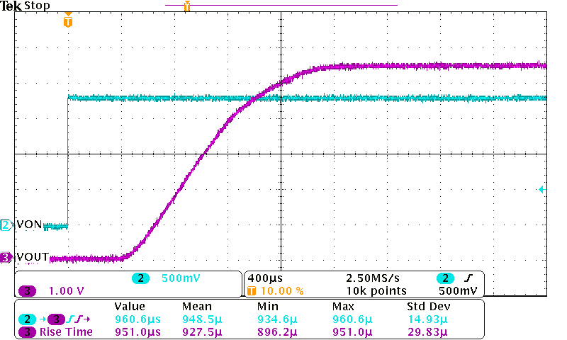
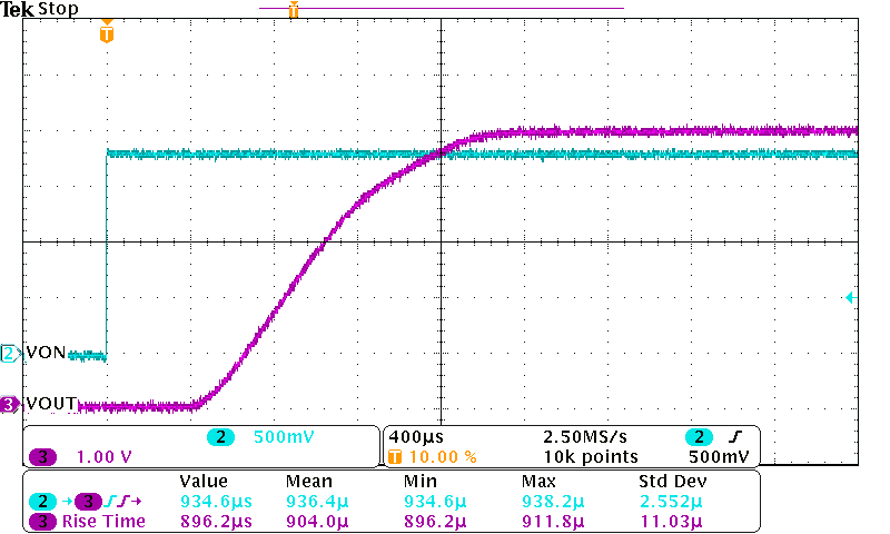
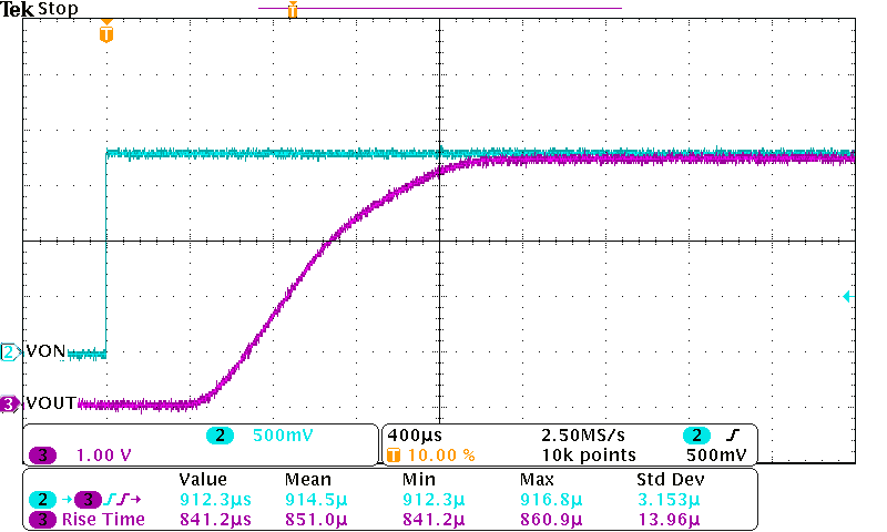
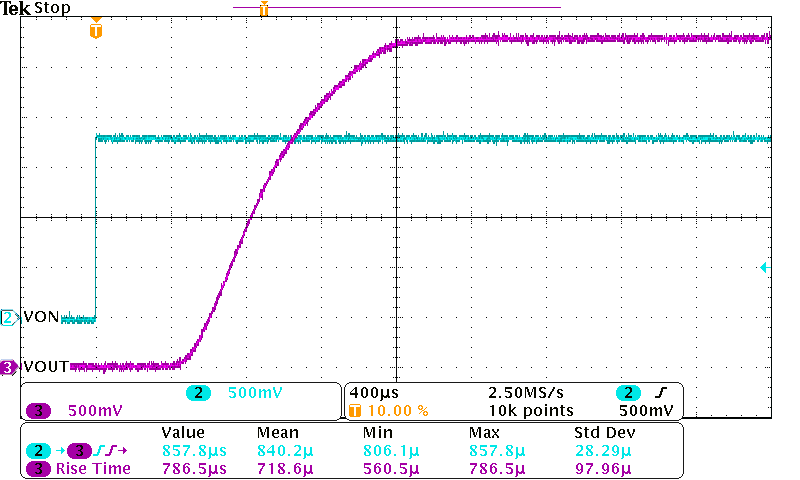
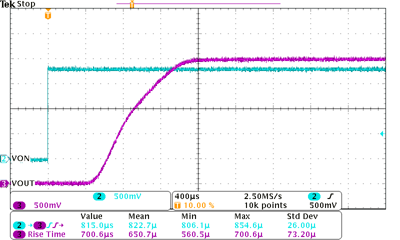
| tON | Turn-ON time | ROUT = 10Ω, CIN = 1µF, COUT = 0.1µF | 928 | µs |
| tOFF | Turn-OFF time | ROUT = 10Ω, CIN = 1µF, COUT = 0.1µF | 2.5 | |
| tR | VOUT rise time | ROUT = 10Ω, CIN = 1µF, COUT = 0.1µF | 890 | |
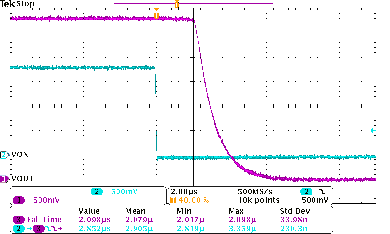
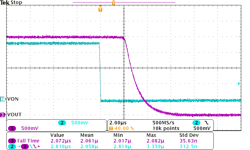
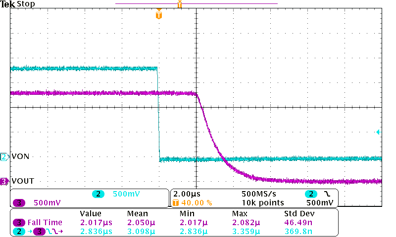
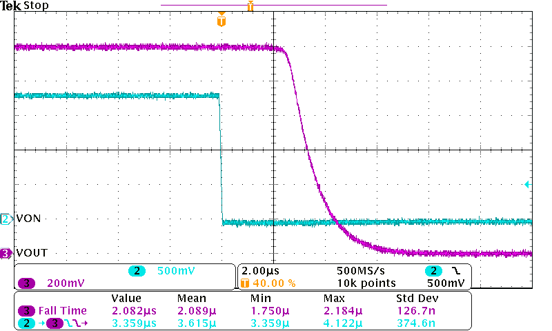
| tF | VOUT fall time | ROUT = 10Ω, CIN = 1µF, COUT = 0.1µF | 2.1 | |
| tD | Delay time | ROUT = 10Ω, CIN = 1µF, COUT = 0.1µF | 561 | |
| VIN = 4.5 V, TA = 25°C (unless otherwise noted) | ||||
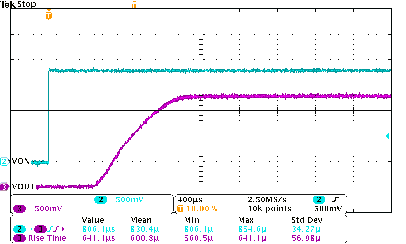
| tON | Turn-ON time | ROUT = 10 Ω, CIN = 1 µF, COUT = 0.1 µF | 905 | µs |
| tOFF | Turn-OFF time | ROUT = 10 Ω, CIN = 1 µF, COUT = 0.1 µF | 2.6 | |
| tR | VOUT rise time | ROUT = 10 Ω, CIN = 1 µF, COUT = 0.1 µF | 859 | |
| tF | VOUT fall time | ROUT = 10 Ω, CIN = 1 µF, COUT = 0.1 µF | 2.1 | |
| tD | Delay time | ROUT = 10 Ω, CIN = 1 µF, COUT = 0.1 µF | 560 | |
| VIN = 3.3 V, TA = 25°C (unless otherwise noted) | ||||
| tON | Turn-ON time | ROUT = 10 Ω, CIN = 1 µF, COUT = 0.1 µF | 836 | µs |
| tOFF | Turn-OFF time | ROUT = 10 Ω, CIN = 1 µF, COUT = 0.1 µF | 2.8 | |
| tR | VOUT rise time | ROUT = 10 Ω, CIN = 1 µF, COUT = 0.1 µF | 715 | |
| tF | VOUT fall time | ROUT = 10 Ω, CIN = 1 µF, COUT = 0.1 µF | 2 | |
| tD | Delay time | ROUT = 10 Ω, CIN = 1 µF, COUT = 0.1 µF | 553 | |
| VIN = 1.8 V, TA = 25°C (unless otherwise noted) | ||||
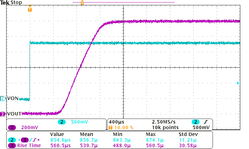
| tON | Turn-ON time | ROUT = 10 Ω, CIN = 1 µF, COUT = 0.1 µF | 822 | µs |
| tOFF | Turn-OFF time | ROUT = 10 Ω, CIN = 1 µF, COUT = 0.1 µF | 2.8 | |
| tR | VOUT rise time | ROUT = 10 Ω, CIN = 1 µF, COUT = 0.1 µF | 651 | |
| tF | VOUT fall time | ROUT = 10 Ω, CIN = 1 µF, COUT = 0.1 µF | 2 | |
| tD | Delay time | ROUT = 10 Ω, CIN = 1 µF, COUT = 0.1 µF | 558 | |
| VIN = 1.2 V, TA = 25°C (unless otherwise noted) | ||||
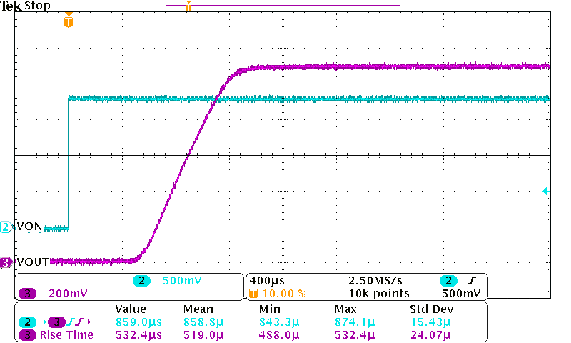
| tON | Turn-ON time | ROUT = 10 Ω, CIN = 1 µF, COUT = 0.1 µF | 852 | µs |
| tOFF | Turn-OFF time | ROUT = 10 Ω, CIN = 1 µF, COUT = 0.1 µF | 3.2 | |
| tR | VOUT rise time | ROUT = 10 Ω, CIN = 1 µF, COUT = 0.1 µF | 535 | |
| tF | VOUT fall time | ROUT = 10 Ω, CIN = 1 µF, COUT = 0.1 µF | 1.8 | |
| tD | Delay time | ROUT = 10 Ω, CIN = 1 µF, COUT = 0.1 µF | 594 | |
| VIN = 1.1 V, TA = 25°C (unless otherwise noted) | ||||
| tON | Turn-ON time | ROUT = 10 Ω, CIN = 1 µF, COUT = 0.1 µF | 861 | µs |
| tOFF | Turn-OFF time | ROUT = 10 Ω, CIN = 1 µF, COUT = 0.1 µF | 3.5 | |
| tR | VOUT rise time | ROUT = 10 Ω, CIN = 1 µF, COUT = 0.1 µF | 518 | |
| tF | VOUT fall time | ROUT = 10 Ω, CIN = 1 µF, COUT = 0.1 µF | 1.9 | |
| tD | Delay time | ROUT = 10 Ω, CIN = 1 µF, COUT = 0.1 µF | 604 | |
8.7 Typical Electrical Characteristics
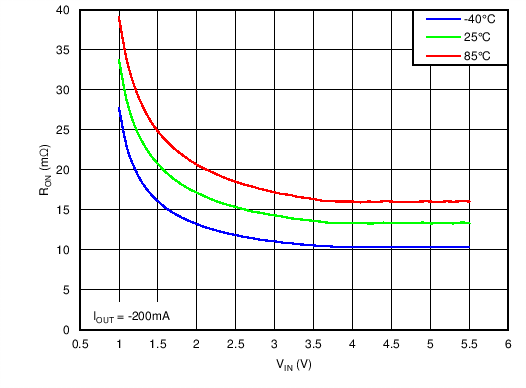 Figure 1. On Resistance vs VIN
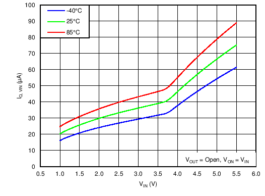 Figure 3. Quiescent Current vs VIN
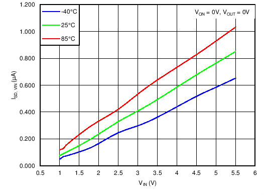 Figure 5. Shut Down Current vs VIN
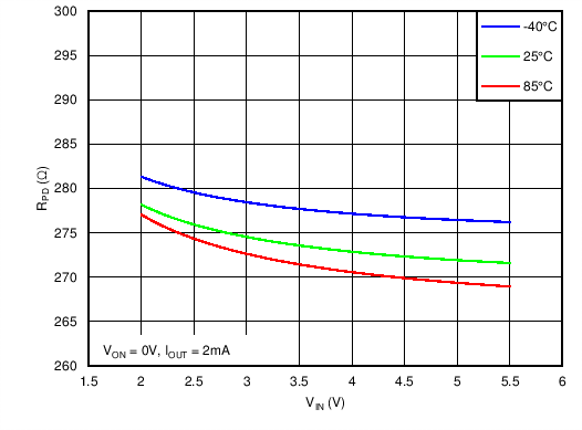 Figure 7. Output Pulldown Resistance vs VIN
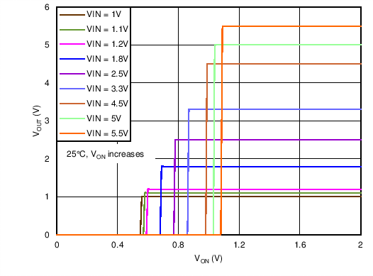 Figure 9. Output Voltage vs VON Rising
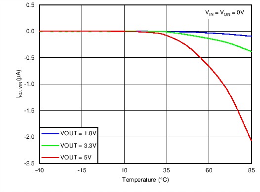 Figure 11. Reverse Current When Disabled vs Temperature
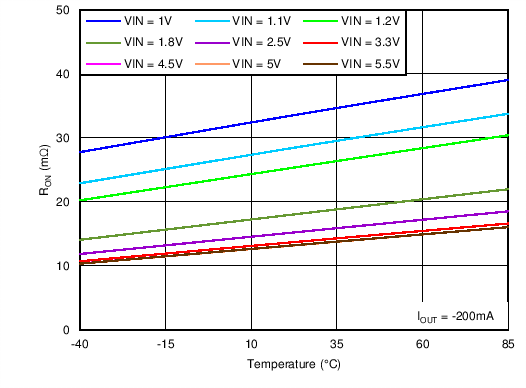 Figure 2. On Resistance vs Temperature
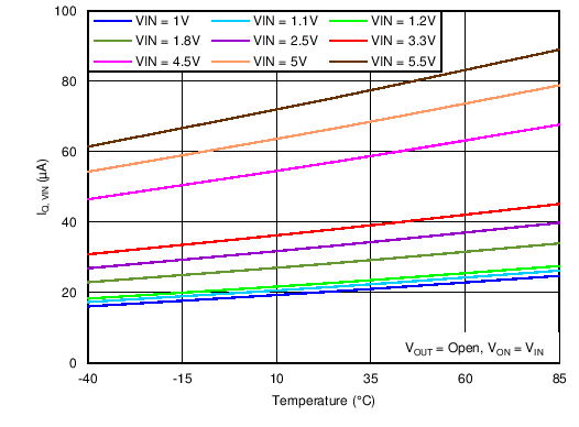 Figure 4. Quiescent Current vs Temperature
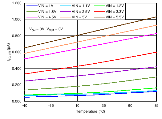 Figure 6. Shut Down Current vs Temperature
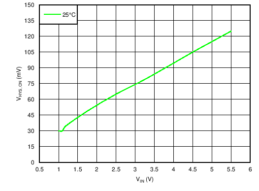 Figure 8. On Pin Hysteresis vs VIN
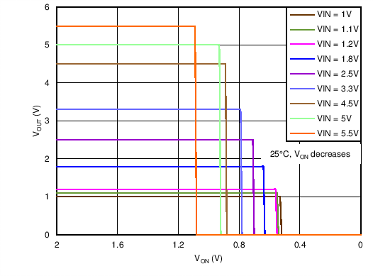 Figure 10. Output Voltage vs VON Falling
8.8 Typical Switching Characteristics
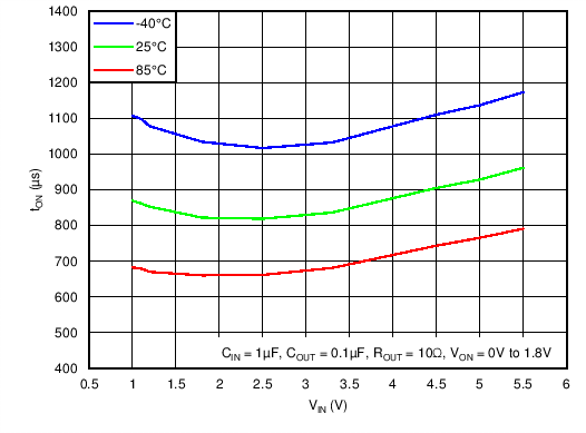 Figure 12. Turn-On Time vs VIN
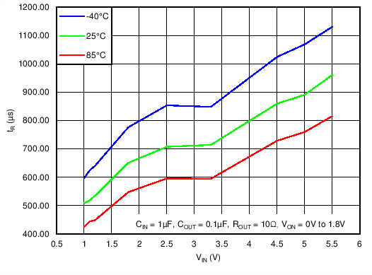 Figure 14. VOUT Rise Time vs VIN
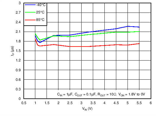 Figure 16. VOUT Fall Time vs VIN
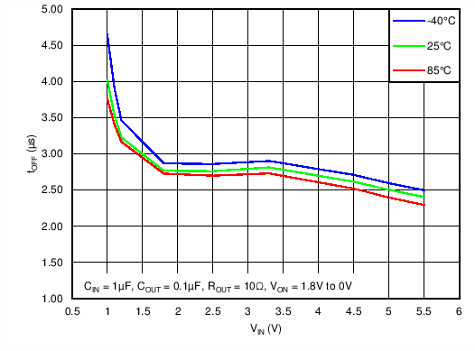 Figure 13. Turn-Off Time vs VIN
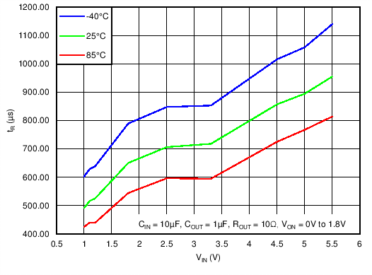 Figure 15. VOUT Rise Time vs VIN
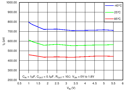 Figure 17. Delay Time vs VIN
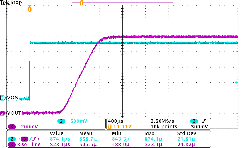
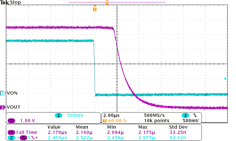
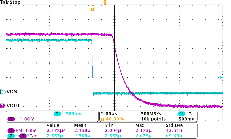
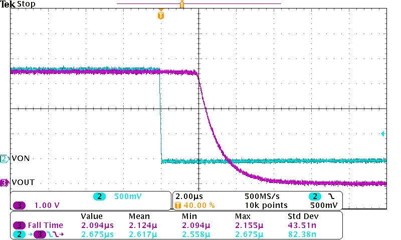
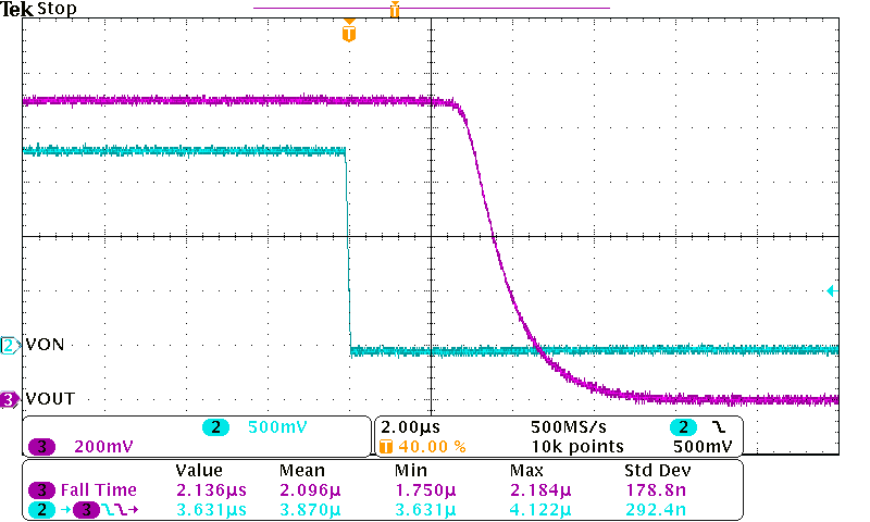
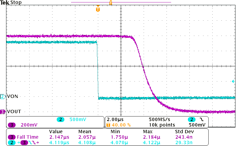
8.9 Typical AC Scope Captures at TA = 25ºC