SLVSCI3E April 2014 – July 2022 TPS22965-Q1
PRODUCTION DATA
- 1 Features
- 2 Applications
- 3 Description
- 4 Revision History
- 5 Device Comparison Table
- 6 Pin Configuration and Functions
- 7 Specifications
- 8 Parameter Measurement Information
- 9 Detailed Description
- 10Application and Implementation
- 11Power Supply Recommendations
- 12Layout
- 13Device and Documentation Support
- 14Mechanical, Packaging, and Orderable Information
Package Options
Mechanical Data (Package|Pins)
- DSG|8
Thermal pad, mechanical data (Package|Pins)
- DSG|8
Orderable Information
3 Description
The TPS22965x-Q1 is a small, ultra-low-RON, single-channel load switch with controlled turn-on. The device contains an N-channel MOSFET that can operate over an input voltage range of 0.8 V to 5.5 V and can support a maximum continuous current of 4 A. The VOUT rise time is configurable so that inrush current can be reduced. The TPS22965-Q1 and TPS22965W-Q1 devices include a 225-Ω on-chip load resistor for quick output discharge when the switch is turned off.
The TPS22965x-Q1 devices are available in a small, space-saving 2-mm × 2-mm 8-pin WSON package (DSG0008A) with integrated thermal pad allowing for high power dissipation. The TPS22965-Q1 and TPS22965N-Q1 devices are characterized for operation over the free-air temperature range of –40°C to 105°C. Furthermore, the TPS22965W-Q1 and TPS22965NW-Q1 devices feature wettable flanks in the same WSON package (DSG0008B) and it is characterized for operation over the free-air temperature range of –40°C to +125°C.
| PART NUMBER | PACKAGE | BODY SIZE (NOM) |
|---|---|---|
| TPS22965-Q1 | DSG0008A WSON (8) |
2.00 mm × 2.00 mm |
| TPS22965N-Q1 | ||
| TPS22965W-Q1 | DSG0008B WSON (8) |
|
| TPS22965NW-Q1 |
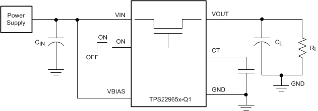
 Simplified Schematic
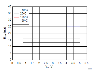
 RON vs VIN
(VBIAS = 5 V, IOUT = –200 mA)