SLVSC71B December   2013  – March 2020 TPS22966-Q1

PRODUCTION DATA.  

  1. Features
  2. Applications
  3. Description
    1.     Device Images
      1.      Typical Application Schematic
  4. Revision History
  5. Pin Configuration and Functions
    1.     Pin Functions
  6. Specifications
    1. 6.1 Absolute Maximum Ratings
    2. 6.2 ESD Ratings
    3. 6.3 Recommended Operating Conditions
    4. 6.4 Thermal Information
    5. 6.5 Electrical Characteristics: VBIAS = 5 V
    6. 6.6 Electrical Characteristics: VBIAS = 2.5 V
    7. 6.7 Switching Characteristics
    8. 6.8 Typical Characteristics
      1. 6.8.1 Typical AC Scope Captures at TA = 25ºC, CT = 1 nF
  7. Parameter Measurement Information
  8. Detailed Description
    1. 8.1 Overview
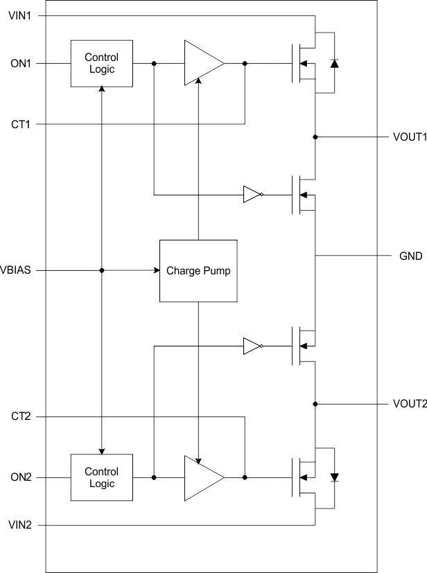
    2. 8.2 Functional Block Diagram
    3. 8.3 Feature Description
      1. 8.3.1 Quick Output Discharge
      2. 8.3.2 ON/OFF Control
      3. 8.3.3 Adjustable Rise Time
    4. 8.4 Device Functional Modes
  9. Application and Implementation
    1. 9.1 Application Information
      1. 9.1.1 Input Capacitor (Optional)
      2. 9.1.2 Output Capacitor (Optional)
      3. 9.1.3 VIN and VBIAS Voltage Range
      4. 9.1.4 Safe Operating Area (SOA)
    2. 9.2 Typical Application
      1. 9.2.1 Design Requirements
      2. 9.2.2 Detailed Design Procedure
      3. 9.2.3 Application Curves
  10. 10Power Supply Recommendations
  11. 11Layout
    1. 11.1 Layout Guidelines
    2. 11.2 Layout Example
  12. 12Device and Documentation Support
    1. 12.1 Trademarks
    2. 12.2 Electrostatic Discharge Caution
    3. 12.3 Glossary
    4. 12.4 Receiving Notification of Documentation Updates
    5. 12.5 Support Resources
  13. 13Mechanical, Packaging, and Orderable Information

Package Options

Mechanical Data (Package|Pins)
Thermal pad, mechanical data (Package|Pins)
Orderable Information

Functional Block Diagram

TPS22966-Q1 fbd_lvsbh4.gif