SLVSDK1C May   2016  – September 2017 TPS22990

PRODUCTION DATA.  

  1. Features
  2. Applications
  3. Description
  4. Revision History
  5. Device Comparison Table
  6. Pin Configuration and Functions
  7. Specifications
    1. 7.1 Absolute Maximum Ratings
    2. 7.2 ESD Ratings
    3. 7.3 Recommended Operating Conditions
    4. 7.4 Thermal Information
    5. 7.5 Electrical Characteristics—VBIAS = 5 V
    6. 7.6 Electrical Characteristics—VBIAS = 3.3 V
    7. 7.7 Switching Characteristics
    8. 7.8 Typical Characteristics
  8. Parameter Measurement Information
  9. Detailed Description
    1. 9.1 Overview
    2. 9.2 Functional Block Diagram
    3. 9.3 Feature Description
      1. 9.3.1 On and Off Control
      2. 9.3.2 Adjustable Rise Time
      3. 9.3.3 Power Good (PG)
      4. 9.3.4 Quick Output Discharge (QOD) (TPS22990 Only)
    4. 9.4 Device Functional Modes
  10. 10Application and Implementation
    1. 10.1 Application Information
      1. 10.1.1 Input to Output Voltage Drop
      2. 10.1.2 Input Capacitor
      3. 10.1.3 Thermal Consideration
      4. 10.1.4 PG Pull Up Resistor
      5. 10.1.5 Power Sequencing
      6. 10.1.6 Standby Power Reduction
    2. 10.2 Typical Application
      1. 10.2.1 Design Requirements
      2. 10.2.2 Detailed Design Procedure
        1. 10.2.2.1 Managing Inrush Current
      3. 10.2.3 Application Curves
  11. 11Power Supply Recommendations
  12. 12Layout
    1. 12.1 Layout Guidelines
    2. 12.2 Layout Example
  13. 13Device and Documentation Support
    1. 13.1 Documentation Support
      1. 13.1.1 Related Documentation
    2. 13.2 Receiving Notification of Documentation Updates
    3. 13.3 Community Resources
    4. 13.4 Trademarks
    5. 13.5 Electrostatic Discharge Caution
    6. 13.6 Glossary
  14. 14Mechanical, Packaging, and Orderable Information

Package Options

Mechanical Data (Package|Pins)
Thermal pad, mechanical data (Package|Pins)
Orderable Information

Parameter Measurement Information

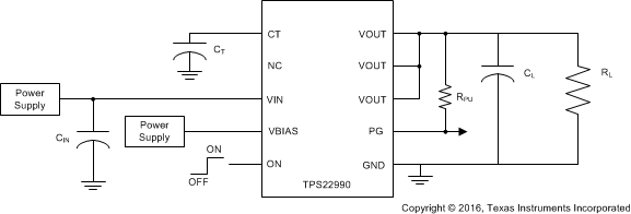
TPS22990 TPS22990_waveform_timing_test_circuit.gif Figure 34. Timing Test Circuit
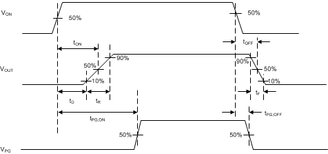
TPS22990 TPS22990_timing_waveform.gif
Rise and fall times of the control signals is 100 ns.
Figure 35. Timing Waveforms