SLVSDF9A December 2017 – January 2019 TPS23523
PRODUCTION DATA.
- 1 Features
- 2 Applications
- 3 Description
- 4 Revision History
- 5 Pin Configuration and Functions
- 6 Specifications
- 7 Parameter Measurement Information
- 8 Detailed Description
-
9 Application and Implementation
- 9.1 Application Information
- 9.2
Typical Application
- 9.2.1 Design Requirements
- 9.2.2
Detailed Design Procedure
- 9.2.2.1 Selecting RSNS
- 9.2.2.2 Selecting Soft Start Setting: CSS and CSS,VEE
- 9.2.2.3 Selecting VDS Switch Over Threshold
- 9.2.2.4 Timer Selection
- 9.2.2.5 MOSFET Selection and SOA Checks
- 9.2.2.6 Input Cap, Input TVS, and OR-ing FET selection
- 9.2.2.7 EMI Filter Consideration
- 9.2.2.8 Undervoltage and Overvoltage Settings
- 9.2.2.9 Choosing RVCC and CVCC
- 9.2.2.10 Power Good Interface to Downstream DC/DC
- 9.2.3 Application Curves
- 10Power Supply Recommendations
- 11Layout
- 12Device and Documentation Support
- 13Mechanical, Packaging, and Orderable Information
Package Options
Mechanical Data (Package|Pins)
- PW|16
Thermal pad, mechanical data (Package|Pins)
Orderable Information
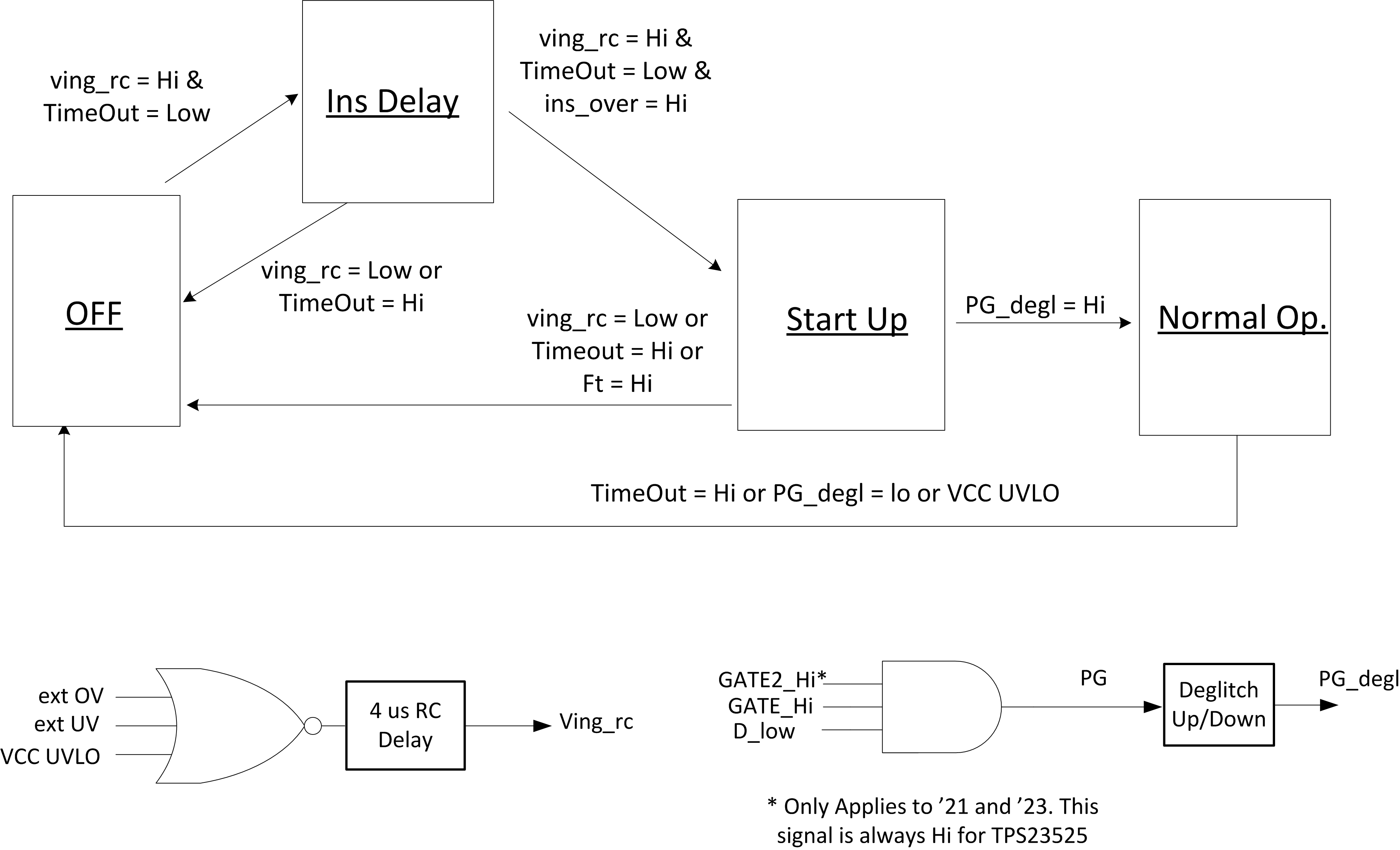
8.4 Device Functional Modes
 Figure 13. Simplified Hot Swap State Machine
 The Figure above shows a simplified state machine of the hot swap controller. It has 4 distinct operating states and the controller switches between these states based on the following signals:
- Ving_rc: This means that both the input voltage is in the right range and the IC has power with Vcc. A 4-µs delay is added for deglitching. If the input voltage is above the OV threshold, input voltage is below the UV threshold, or VCC is below its internal UVLO, Ving_rc will be low.
- TimeOut: This signal comes from the timer block and will be asserted Hi if the IC has timed out due to an over-current condition. This signal is also Hi while the timer is going through the restart cycles. Once the cycles are completed this signal will go Low.
- ins_over: This signal states that the insertion delay has been completed and the hot swap is ready to start-up.
- FT: this is the fast trip signal coming from the fast trip comparator. It goes Hi if an extreme over current event is detected.
- PG: Internal Power good signal. This is high when the hot swap is fully on and the load can draw full power. For PG to be Hi, the GATE has to be Hi, GATE2 needs to be Hi, and the drain pin needs to be below 0.75 V.
- PG_degl: This is a deglitched version of the PG and is the signal used to move between states and controls the external PGb pin.