SLVSDF9A December 2017 – January 2019 TPS23523
PRODUCTION DATA.
- 1 Features
- 2 Applications
- 3 Description
- 4 Revision History
- 5 Pin Configuration and Functions
- 6 Specifications
- 7 Parameter Measurement Information
- 8 Detailed Description
-
9 Application and Implementation
- 9.1 Application Information
- 9.2
Typical Application
- 9.2.1 Design Requirements
- 9.2.2
Detailed Design Procedure
- 9.2.2.1 Selecting RSNS
- 9.2.2.2 Selecting Soft Start Setting: CSS and CSS,VEE
- 9.2.2.3 Selecting VDS Switch Over Threshold
- 9.2.2.4 Timer Selection
- 9.2.2.5 MOSFET Selection and SOA Checks
- 9.2.2.6 Input Cap, Input TVS, and OR-ing FET selection
- 9.2.2.7 EMI Filter Consideration
- 9.2.2.8 Undervoltage and Overvoltage Settings
- 9.2.2.9 Choosing RVCC and CVCC
- 9.2.2.10 Power Good Interface to Downstream DC/DC
- 9.2.3 Application Curves
- 10Power Supply Recommendations
- 11Layout
- 12Device and Documentation Support
- 13Mechanical, Packaging, and Orderable Information
Package Options
Mechanical Data (Package|Pins)
- PW|16
Thermal pad, mechanical data (Package|Pins)
Orderable Information
8.3.4 Gate 2
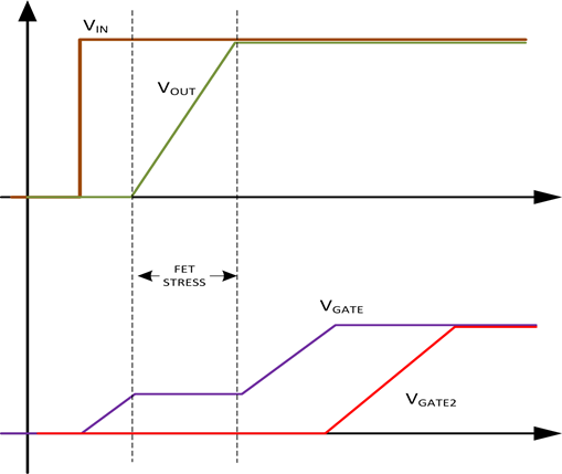
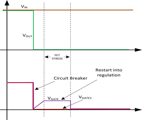
The TPS23523 features a second hot swap Gate drive, which can be used to save BOM cost and size in applications that require multiple hot swap MOSFETs. The 2nd MOSFET is only turned ON when the main FET is enhanced. As a result the 2nd MOSFET doesn't operate with large current and large voltage across it, thus reducing the SOA requirements. In many cases a 5x6 QFN FET can replace a D2PACK FET. The following figures show the operation during start-up and Hot Short event. It can be seen that the second FET is OFF during stressful operation and turns on during normal operation to improve steady state efficiency and reduce power losses.
 Figure 10. Gate 2 Operation During Start-Up
  Figure 11. Gate2 Operation During Hot Short