SLUSCM4B October 2017 – November 2018 TPS2372
PRODUCTION DATA.
- 1 Features
- 2 Applications
- 3 Description
- 4 Revision History
- 5 Pin Configuration and Functions
- 6 Specifications
-
7 Detailed Description
- 7.1 Overview
- 7.2 Functional Block Diagram
- 7.3
Feature Description
- 7.3.1 PG Power Good (Converter Enable) Pin Interface
- 7.3.2 CLSA and CLSB Classification, AUTCLS
- 7.3.3 DEN Detection and Enable
- 7.3.4 Internal Pass MOSFET and Inrush Delay Enable, IRSHDL_EN
- 7.3.5 TPH, TPL and BT PSE Type Indicators
- 7.3.6 AMPS_CTL, MPS_DUTY and Automatic MPS
- 7.3.7 VDD Supply Voltage
- 7.3.8 VSS
- 7.3.9 Exposed Thermal PAD
- 7.4
Device Functional Modes
- 7.4.1 PoE Overview
- 7.4.2 Threshold Voltages
- 7.4.3 PoE Startup Sequence
- 7.4.4 Detection
- 7.4.5 Hardware Classification
- 7.4.6 Autoclass
- 7.4.7 Inrush and Startup
- 7.4.8 Maintain Power Signature
- 7.4.9 Startup and Converter Operation
- 7.4.10 PD Hotswap Operation
- 7.4.11 Startup and Power Management, PG and TPH, TPL, BT
- 7.4.12 Using DEN to Disable PoE
-
8 Application and Implementation
- 8.1 Application Information
- 8.2
Typical Application
- 8.2.1 Design Requirements
- 8.2.2
Detailed Design Requirements
- 8.2.2.1 Input Bridges and Schottky Diodes
- 8.2.2.2 Protection, D1
- 8.2.2.3 Capacitor, C1
- 8.2.2.4 Detection Resistor, RDEN
- 8.2.2.5 Classification Resistors, RCLSA and RCLSB
- 8.2.2.6 Opto-isolators for TPH, TPL and BT
- 8.2.2.7 Automatic MPS and MPS Duty Cycle, RMPS and RMPS_DUTY
- 8.2.2.8 Internal Voltage Reference, RREF
- 8.2.2.9 Autoclass
- 8.2.2.10 Inrush Delay
- 8.2.3 Application Curves
- 9 Power Supply Recommendations
- 10Layout
- 11Device and Documentation Support
- 12Mechanical, Packaging, and Orderable Information
Package Options
Refer to the PDF data sheet for device specific package drawings
Mechanical Data (Package|Pins)
- RGW|20
Thermal pad, mechanical data (Package|Pins)
Orderable Information
7.4.2 Threshold Voltages
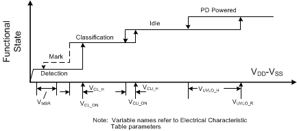
The TPS2372 has a number of internal comparators with hysteresis for stable switching between the various states. Figure 16 relates the parameters in Electrical Characteristics to the PoE states. The mode labeled Idle between Classification and Operation implies that the DEN, CLSA, CLSB, and RTN pins are all high impedance. The state labeled Mark, which is drawn in dashed lines, is part of the Type 2-3-4 hardware class state machine.
 Figure 16. Threshold Voltages