SLUSCM4B October   2017  – November 2018 TPS2372

PRODUCTION DATA.  

  1. Features
  2. Applications
  3. Description
    1.     Device Images
      1.      Simplified Schematic
  4. Revision History
  5. Pin Configuration and Functions
    1.     Pin Functions
  6. Specifications
    1. 6.1 Absolute Maximum Ratings
    2. 6.2 ESD Ratings
    3. 6.3 Recommended Operating Conditions
    4. 6.4 Thermal Information
    5. 6.5 Electrical Characteristics
    6. 6.6 Typical Characteristics
  7. Detailed Description
    1. 7.1 Overview
    2. 7.2 Functional Block Diagram
    3. 7.3 Feature Description
      1. 7.3.1 PG Power Good (Converter Enable) Pin Interface
      2. 7.3.2 CLSA and CLSB Classification, AUTCLS
      3. 7.3.3 DEN Detection and Enable
      4. 7.3.4 Internal Pass MOSFET and Inrush Delay Enable, IRSHDL_EN
      5. 7.3.5 TPH, TPL and BT PSE Type Indicators
      6. 7.3.6 AMPS_CTL, MPS_DUTY and Automatic MPS
      7. 7.3.7 VDD Supply Voltage
      8. 7.3.8 VSS
      9. 7.3.9 Exposed Thermal PAD
    4. 7.4 Device Functional Modes
      1. 7.4.1  PoE Overview
      2. 7.4.2  Threshold Voltages
      3. 7.4.3  PoE Startup Sequence
      4. 7.4.4  Detection
      5. 7.4.5  Hardware Classification
      6. 7.4.6  Autoclass
      7. 7.4.7  Inrush and Startup
      8. 7.4.8  Maintain Power Signature
      9. 7.4.9  Startup and Converter Operation
      10. 7.4.10 PD Hotswap Operation
      11. 7.4.11 Startup and Power Management, PG and TPH, TPL, BT
      12. 7.4.12 Using DEN to Disable PoE
  8. Application and Implementation
    1. 8.1 Application Information
    2. 8.2 Typical Application
      1. 8.2.1 Design Requirements
      2. 8.2.2 Detailed Design Requirements
        1. 8.2.2.1  Input Bridges and Schottky Diodes
        2. 8.2.2.2  Protection, D1
        3. 8.2.2.3  Capacitor, C1
        4. 8.2.2.4  Detection Resistor, RDEN
        5. 8.2.2.5  Classification Resistors, RCLSA and RCLSB
        6. 8.2.2.6  Opto-isolators for TPH, TPL and BT
        7. 8.2.2.7  Automatic MPS and MPS Duty Cycle, RMPS and RMPS_DUTY
        8. 8.2.2.8  Internal Voltage Reference, RREF
        9. 8.2.2.9  Autoclass
        10. 8.2.2.10 Inrush Delay
      3. 8.2.3 Application Curves
  9. Power Supply Recommendations
  10. 10Layout
    1. 10.1 Layout Guidelines
    2. 10.2 Layout Example
    3. 10.3 EMI Containment
    4. 10.4 Thermal Considerations and OTSD
    5. 10.5 ESD
  11. 11Device and Documentation Support
    1. 11.1 Documentation Support
      1. 11.1.1 Related Links
      2. 11.1.2 Related Documentation
    2. 11.2 Receiving Notification of Documentation Updates
    3. 11.3 Community Resources
    4. 11.4 Trademarks
    5. 11.5 Electrostatic Discharge Caution
    6. 11.6 Glossary
  12. 12Mechanical, Packaging, and Orderable Information

Package Options

Refer to the PDF data sheet for device specific package drawings

Mechanical Data (Package|Pins)
  • RGW|20
Thermal pad, mechanical data (Package|Pins)
Orderable Information

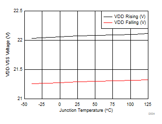
Typical Characteristics

TPS2372 D001_SLUSCD1.gif
Figure 1. Detection Bias Current vs PoE Voltage
TPS2372 D003_SLUSCD1.gif
Figure 3. Classification Lower Threshold vs Temperature
TPS2372 D005_SLUSCD1.gif
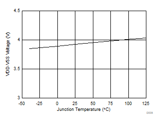
Figure 5. Mark Reset Threshold vs Temperature
TPS2372 D008_SLUSCD1.gif
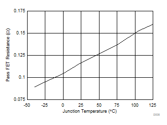
Figure 7. Pass FET Resistance vs Temperature, TPS2372-4
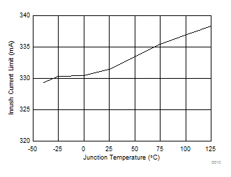
TPS2372 D010_SLUSCD1.gif
Figure 9. PoE Inrush Current Limit vs Temperature, TPS2372-4
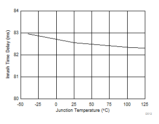
TPS2372 D012_SLUSCD1.gif
Figure 11. Inrush Time Delay vs Temperature
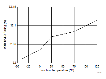
TPS2372 D014_SLUSCD1.gif
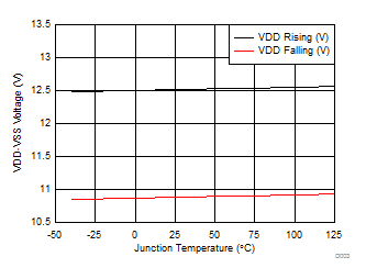
Figure 13. UVLO Falling Threshold vs Temperature
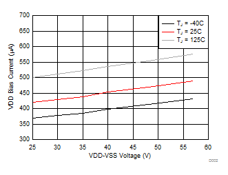
TPS2372 D002_SLUSCD1.gif
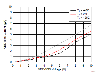
Figure 2. IVDD Bias Current vs Voltage
TPS2372 D004_SLUSCD1.gif
Figure 4. Classification Upper Threshold vs Temperature
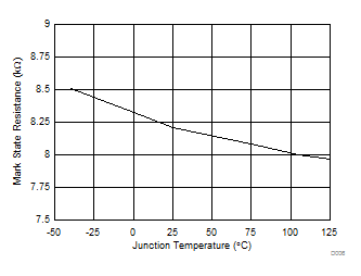
TPS2372 D006_SLUSCD1.gif
Figure 6. Mark Resistance vs Temperature
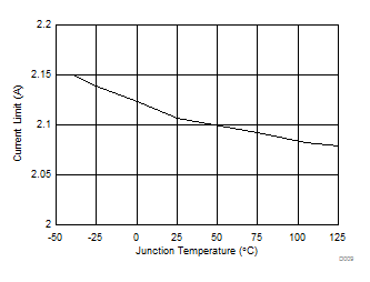
TPS2372 D009_SLUSCD1.gif
Figure 8. PoE Current Limit vs Temperature, TPS2372-4
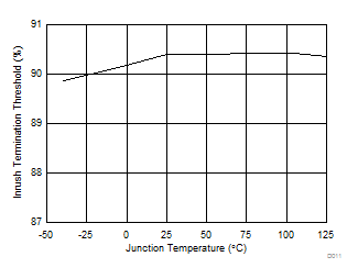
TPS2372 D011_SLUSCD1.gif
Figure 10. Inrush Termination Threshold vs Temperature, TPS2372-4
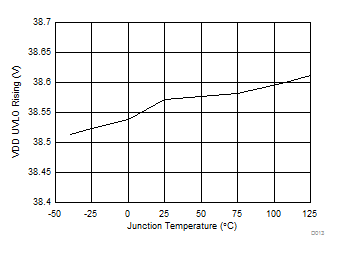
TPS2372 D013_SLUSCD1.gif
Figure 12. UVLO Rising Threshold vs Temperature