SLUS907K January   2009  – June 2019 TPS2421-1 , TPS2421-2

PRODUCTION DATA.  

  1. Features
  2. Applications
  3. Description
    1.     Device Images
      1.      Typical Application
  4. Revision History
  5. Device Comparison Table
  6. Pin Configuration and Functions
    1.     Pin Functions
  7. Specifications
    1. 7.1 Absolute Maximum Ratings
    2. 7.2 ESD Ratings
    3. 7.3 Recommended Operating Conditions
    4. 7.4 Thermal Information
    5. 7.5 Electrical Characteristics
    6. 7.6 Typical Characteristics
  8. Detailed Description
    1. 8.1 Overview
    2. 8.2 Functional Block Diagram
    3. 8.3 Feature Description
      1. 8.3.1 CT
      2. 8.3.2 FLT
      3. 8.3.3 GND
      4. 8.3.4 ISET
      5. 8.3.5 VIN
      6. 8.3.6 VOUT
      7. 8.3.7 PG
    4. 8.4 Device Functional Modes
      1. 8.4.1 Startup
      2. 8.4.2 Maximum Allowable Load to Ensure Successful Startup
        1. 8.4.2.1 Enable Pin Considerations
        2. 8.4.2.2 Fault Timer
        3. 8.4.2.3 Normal Operation
        4. 8.4.2.4 Startup into a Short
      3. 8.4.3 Shutdown Modes
        1. 8.4.3.1 Hard Overload - Fast Trip
        2. 8.4.3.2 Overcurrent Shutdown
    5. 8.5 Programming
      1. 8.5.1 Fault (ISET) and Current-Limit (ILIM) Thresholds
  9. Application and Implementation
    1. 9.1 Application Information
    2. 9.2 Typical Application
      1. 9.2.1 Design Requirements
      2. 9.2.2 Detailed Design Procedure
        1. 9.2.2.1 Transient Protection
      3. 9.2.3 Application Curves
  10. 10Power Supply Recommendations
    1. 10.1 PowerPad™
  11. 11Layout
    1. 11.1 Layout Guidelines
    2. 11.2 Layout Example
  12. 12Device and Documentation Support
    1. 12.1 Documentation Support
      1. 12.1.1 Related Documentation
    2. 12.2 Related Links
    3. 12.3 Receiving Notification of Documentation Updates
    4. 12.4 Community Resource
    5. 12.5 Trademarks
    6. 12.6 Electrostatic Discharge Caution
    7. 12.7 Glossary
  13. 13Mechanical, Packaging, and Orderable Information

Package Options

Mechanical Data (Package|Pins)
Thermal pad, mechanical data (Package|Pins)
Orderable Information

Enable Pin Considerations

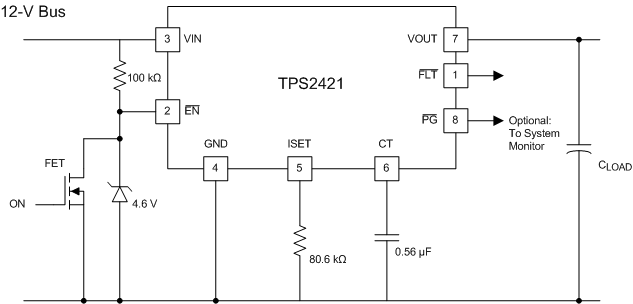
For the case when EN is simply connected to GND, the TPS2421 device starts ramping the voltage on VOUT as VIN rises above UVLO (approximately 2.85 V typical). If IN does not ramp monotonically, the TPS2421 may momentarily turnoff then on during startup if IN falls below approximately 2.7 V. To avoid this problem, EN assertion can be delayed until IN is sufficiently above UVLO. A simple approach is shown in Figure 12. The 100-kΩ pullup resistor de-asserts EN when VIN is above approximately 1.75 V maximum which is well below the minimum UVLO of approximately 2.6 V. The Zener diode ensures that EN remains below 5 V. User control to enable the TPS2421 device is applied at the ON node to turn on the FET once IN has risen sufficiently above UVLO.
TPS2421-1 TPS2421-2 EN_del_cir_lus907.gifFigure 12. EN Delay Circuit