SLVSBY8D May 2013 – June 2020 TPS2513 , TPS2513A , TPS2514 , TPS2514A
PRODUCTION DATA.
- 1 Features
- 2 Applications
- 3 Description
- 4 Revision History
- 5 Device Options
- 6 Pin Configuration and Functions
- 7 Specifications
- 8 Detailed Description
- 9 Applications and Implementation
- 10Power Supply Recommendations
- 11Layout
- 12Device and Documentation Support
- 13Mechanical, Packaging, and Orderable Information
Package Options
Mechanical Data (Package|Pins)
- DBV|6
Thermal pad, mechanical data (Package|Pins)
Orderable Information
8.3.5 DCP Auto-Detect
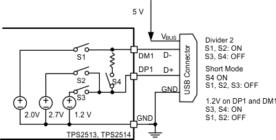
The devices integrate an auto-detect feature to support divider mode, short mode and 1.2 V / 1.2 V modes. If a divider device is attached, 2.7 V is applied to the DP pin and 2 V is applied to the DM pin. If a BC1.2-compliant device is attached, the TPS2513 and TPS2514 automatically switches into short mode. If a device compliant with the 1.2 V / 1.2 V charging scheme is attached, 1.2 V is applied on both the DP pin and the DM pin. The functional diagram of DCP auto-detect feature (DM1 and DP1) is shown in Figure 15. DCP auto-detect feature (DM2 and DP2 of TPS2513) has the same functional configuration. For TPS2513A and TPS2514A, the devices also have DCP auto-detect feature and the auto-detect have the same functional configuration expect for the default mode is Divider 3 (D+/D– = 2.7 V / 2.7 V).
 Figure 15. TPS2513 and TPS2514 DCP Auto-Detect Functional Diagram