SLVS736C February 2008 – October 2023 TPS2550 , TPS2551
PRODUCTION DATA
- 1
- 1 Features
- 2 Applications
- 3 Description
- 4 Revision History
- 5 Device Comparison Table
- 6 Pin Configuration and Functions
- 7 Specifications
- 8 Parameter Measurement Information
- 9 Detailed Description
-
10Application and Implementation
- 10.1 Application Information
- 10.2 Typical Applications
- 10.3 Power Supply Recommendations
- 10.4 Layout
- 11Device and Documentation Support
- 12Mechanical, Packaging, and Orderable Information
Package Options
Mechanical Data (Package|Pins)
Thermal pad, mechanical data (Package|Pins)
- DRV|6
Orderable Information
6 Pin Configuration and Functions
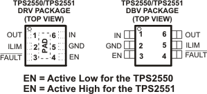
Table 6-1 Pin Functions
| PIN | I/O | DESCRIPTION | ||||
|---|---|---|---|---|---|---|
| NAME | TPS2550DBV | TPS2551DBV | TPS2550DRV | TPS2551DRV | ||
| EN | 3 | – | 4 | – | I | Enable input, logic low turns on power switch |
| EN | – | 3 | – | 4 | I | Enable input, logic high turns on power switch |
| GND | 2 | 2 | 5 | 5 | Connect ground connection externally to POWER PAD | |
| IN | 1 | 1 | 6 | 6 | I | Input voltage; connect a 0.1 μF or greater ceramic capacitor from IN to GND as close to the IC as possible. |
| FAULT | 4 | 4 | 3 | 3 | O | Active-low open-drain output, asserted during overcurrent, overtemperature, or reverse-voltage conditions. |
| OUT | 6 | 6 | 1 | 1 | O | Power-switch output |
| ILIM | 5 | 5 | 2 | 2 | I | External resistor used to set current-limit threshold; recommended 14.3 kΩ ≤ RILIM ≤ 80.6 kΩ. |
| PowerPAD™ | – | – | PAD | PAD | Internally connected to GND; used to heat-sink the part to the circuit board traces, connect to GND pin. | |