SLVSD03 December 2015 TPS2559-Q1
PRODUCTION DATA.
- 1 Features
- 2 Applications
- 3 Description
- 4 Revision History
- 5 Device Comparison Table
- 6 Pin Configuration and Functions
- 7 Specifications
- 8 Parameter Measurement Information
- 9 Detailed Description
-
10Application and Implementation
- 10.1 Application Information
- 10.2
Typical Application
- 10.2.1 Design Requirements
- 10.2.2
Detailed Design Procedure
- 10.2.2.1 Step by Step Design Procedure
- 10.2.2.2 Input and Output Capacitance
- 10.2.2.3 Programming the Current-Limit Threshold
- 10.2.2.4 Design Above a Minimum Current Limit
- 10.2.2.5 Design Below a Maximum Current Limit
- 10.2.2.6 Accounting for Resistor Tolerance
- 10.2.2.7 Power Dissipation and Junction Temperature
- 10.2.2.8 Auto-Retry
- 10.2.2.9 Two-level Current-limit
- 10.2.3 Application Curves
- 11Power Supply Recommendations
- 12Layout
- 13Device and Documentation Support
- 14Mechanical, Packaging, and Orderable Information
Package Options
Refer to the PDF data sheet for device specific package drawings
Mechanical Data (Package|Pins)
- DRC|10
Thermal pad, mechanical data (Package|Pins)
- DRC|10
Orderable Information
10 Application and Implementation
NOTE
Information in the following applications sections is not part of the TI component specification, and TI does not warrant its accuracy or completeness. TI’s customers are responsible for determining suitability of components for their purposes. Customers should validate and test their design implementation to confirm system functionality.
10.1 Application Information
The TPS2559-Q1 current limited power switch uses N-channel MOSFETs in applications requiring up to 5.5 A of continuous load current. The device enters constant-current mode when the load exceeds the current limit threshold.
The TPS2559-Q1 power switch is used to protect the up-stream power supply when the output is overloaded.
10.2 Typical Application
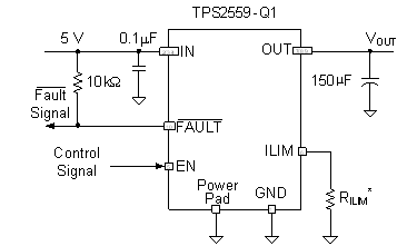 Figure 16. Typical TPS2559-Q1 Power Switch
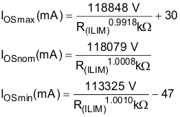
Use the IOS in the Electrical Characteristics table or IOS in Equation 1 to select the RILIM.
10.2.1 Design Requirements
For this design example, use the following as the input parameters.
| DESIGN PARAMETERS | EXAMPLE VALUE |
|---|---|
| Input Operation Voltage | 5 V |
| Rating Current | 3A or 4.5A |
| Minimum Current Limit | 3A |
| Maximum Current Limit | 5A |
When choose power switch, there are some several general steps:
- What is the power rail, 3.3 V or 5 V, and then choose the operation range of power switch can cover the power rail.
- What is the normal operation current, for example, the maximum allowable current drawn by portable equipment for USB 2.0 port is 500mA, so the normal operation current is 500mA and the minimum current limit of power switch must exceed 500 mA to avoid false trigger during normal operation.
- What is the maximum allowable current provided by up-stream power, and then decide the maximum current limit of power switch that must lower it to ensure power switch can protect the up-stream power when over-load is encountered at the output of power switch.
NOTE
Choosing power switch with tighter current limit tolerance can loosen the up-stream power supply design.
10.2.2 Detailed Design Procedure
10.2.2.1 Step by Step Design Procedure
To begin the design process a few parameters must be decided upon. The designer needs to know the following:
- Normal Input Operation Voltage
- Rating Current
- Minimum Current Limit
- Maximum Current Limit
10.2.2.2 Input and Output Capacitance
Input and output capacitance improves the performance of the device; the actual capacitance should be optimized for the particular application. For all applications, a 0.1μF or greater ceramic bypass capacitor between IN and GND is recommended as close to the device as possible for local noise decoupling. This precaution reduces ringing on the input due to power-supply transients. Additional input capacitance may be needed on the input to reduce voltage undershoot from exceeding the UVLO of other load share one power rail with TPS2559-Q1 or overshoot from exceeding the absolute-maximum voltage of the device during heavy transient conditions. This is especially important during bench testing when long, inductive cables are used to connect the evaluation board to the bench power supply.
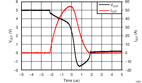
Output capacitance is not required, but placing a high-value electrolytic capacitor on the output pin is recommended when large transient currents are expected on the output to reduce the undershoot, which caused by the inductance of the output power bus just after a short has occurred and the TPS2559-Q1 has abruptly reduced OUT current. Energy stored in the inductance will drive the OUT voltage down and potentially negative as it discharges.
10.2.2.3 Programming the Current-Limit Threshold
The overcurrent threshold is user programmable via an external resistor. The TPS2559-Q1 uses an internal regulation loop to provide a regulated voltage on the ILIM pin. The current-limit threshold is proportional to the current sourced out of ILIM. The recommended 1% resistor range for R(ILIM) is 24.9 kΩ ≤ R(ILIM) ≤ 100 kΩ to ensure stability of the internal regulation loop.
When ILIM pin short to GND (single point failure), maximum current limit is less than 8 A over temperature and process variation.
Many applications require that the minimum current limit is above a certain current level or that the maximum current limit is below a certain current level, so it is important to consider the tolerance of the overcurrent threshold when selecting a value for R(ILIM). The equations and the graph below can be used to estimate the minimum and maximum variation of the current-limit threshold for a predefined resistor value within R(ILIM) is 24.9 kΩ ≤ R(ILIM) ≤ 100 kΩ. This variation is an approximation only and does not take into account, for example, the resistor tolerance. For examples of more-precise variation of IOS refer to the current-limit section of the Electrical Characteristics table.
24.9 kΩ ≤ R(ILIM) ≤ 100 kΩ
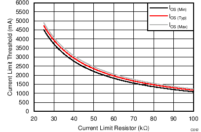 Figure 17. Current-Limit vs R(ILIM)
10.2.2.4 Design Above a Minimum Current Limit
Some applications require that current limiting cannot occur below a certain threshold. For this example, assume that 3 A must be delivered to the load so that the minimum desired current-limit threshold is 3000 mA. Use the IOS equations and Figure 17 to select R(ILIM).

Select the closest 1% resistor less than the calculated value: R(ILIM) = 36.5 kΩ. This sets the minimum current-limit threshold at 3016 A.

Use the IOS equations, Figure 17, and the previously calculated value for R(ILIM) to calculate the maximum resulting current-limit threshold.

The resulting maximum current-limit threshold minimum is 3016 mA and maximum is 3417 mA with a 36.5 kΩ ± 1%.
10.2.2.5 Design Below a Maximum Current Limit
Some applications require that current limiting must occur below a certain threshold. For this example, assume that 5A must be delivered to the load so that the minimum desired current-limit threshold is 5000 mA. Use the IOS equations and Figure 17 to select R(ILIM).

Select the closest 1% resistor less than the calculated value: RILIM = 24.9 kΩ. This sets the maximum current-limit threshold at 4950 A.

Use the IOS equations, Figure 17, and the previously calculated value for R(ILIM) to calculate the minimum resulting current-limit threshold.

The resulting minimum current-limit threshold minimum is 4445 mA and maximum is 4980 mA with a 24.9 kΩ ± 1%.
10.2.2.6 Accounting for Resistor Tolerance
The previous sections described the selection of R(ILIM) given certain application requirements and the importance of understanding the current-limit threshold tolerance. The analysis focused only on the TPS2559-Q1 is bounded by an upper and lower tolerance centered on a nominal resistance. The additional RILIM resistance tolerance directly affects the current-limit threshold accuracy at a system level. Table 1 shows a process that accounts for worst-case resistor tolerance assuming 1% resistor values.
Step one follows the selection process outlined in the application examples above.
Step two determines the upper and lower resistance bounds of the selected resistor.
Step three uses the upper and lower resistor bounds in the IOS equations to calculate the threshold limits.
It is important to use tighter tolerance resistors, that is, 0.5% or 0.1%, when precision current limiting is desired.
Table 1. Common R(ILIM) Resistor Selections
| DESIRED NOMINAL CURRENT LIMIT (mA) |
IDEAL RESISTOR (kΩ) |
CLOSEST 1% RESISTOR (kΩ) |
RESISTOR TOLERANCE | ACTUAL LIMITS | |||||
|---|---|---|---|---|---|---|---|---|---|
| 1% LOW (kΩ) |
1% HIGH (kΩ) |
IOS MIN (mA) |
IOS NOM (mA) |
IOS MAX (mA) |
|||||
| 1250 | 94.1 | 93.1 | 92.2 | 94 | 1152.7 | 1263.7 | 1368.2 | ||
| 1500 | 78.4 | 78.7 | 77.9 | 79.5 | 1372.5 | 1495.1 | 1610.9 | ||
| 1750 | 67.2 | 66.5 | 65.8 | 67.2 | 1633.2 | 1769.7 | 1893.3 | ||
| 2000 | 58.8 | 59 | 58.4 | 59.6 | 1847 | 1994.8 | 2133.7 | ||
| 2250 | 52.3 | 52.3 | 51.8 | 52.8 | 2089.9 | 2550.6 | 2400.9 | ||
| 2500 | 47.1 | 47.5 | 47 | 48 | 2306 | 2478.2 | 2638.4 | ||
| 2750 | 42.8 | 43.2 | 42.8 | 43.6 | 2540.5 | 2725.1 | 2895.8 | ||
| 3000 | 39.2 | 39.2 | 38.8 | 39.6 | 2804.8 | 3003.4 | 3185.7 | ||
| 3250 | 36.2 | 36.5 | 36.1 | 36.9 | 3016 | 3225.7 | 3417.2 | ||
| 3500 | 33.6 | 34 | 33.7 | 34.3 | 3241.4 | 3463.1 | 3664.1 | ||
| 3750 | 31.4 | 31.6 | 31.3 | 31.9 | 3491.5 | 3726.4 | 3937.8 | ||
| 4000 | 29.4 | 29.4 | 29.1 | 29.7 | 3756.5 | 4005.4 | 4227.7 | ||
| 4250 | 27.7 | 28 | 27.7 | 28.3 | 3946.9 | 4205.9 | 4435.8 | ||
| 4500 | 26.2 | 26.1 | 25.8 | 26.4 | 4237.9 | 4512.3 | 4753.9 | ||
| 4750 | 24.8 | 24.9 | 24.7 | 25.1 | 4444.6 | 4729.9 | 4979.6 | ||
10.2.2.7 Power Dissipation and Junction Temperature
The low on-resistance of the N-channel MOSFET allows small surface-mount packages to pass large currents. It is good design practice to estimate power dissipation and junction temperature. The below analysis gives an approximation for calculating junction temperature based on the power dissipation in the package. However, it is important to note that thermal analysis is strongly dependent on additional system level factors. Such factors include air flow, board layout, copper thickness and surface area, and proximity to other devices dissipating power. Good thermal design practice must include all system level factors in addition to individual component analysis. Begin by determining the rDS(on) of the N-channel MOSFET relative to the input voltage and operating temperature. As an initial estimate, use the highest operating ambient temperature of interest and read rDS(on) from the typical characteristics graph. Using this value, the power dissipation can be calculated using Equation 8:
Where:
PD = Total power dissipation (W)
rDS(on) = Power switch on-resistance (Ω)
IOUT = Maximum current-limit threshold (A)
This step calculates the total power dissipation of the N-channel MOSFET.
Finally, calculate the junction temperature:
Where:
TA = Ambient temperature (°C)
θJA = Thermal resistance (°C/W)
PD = Total power dissipation (W)
Compare the calculated junction temperature with the initial estimate. If they are not within a few degrees, repeat the calculation using the "refined" rDS(on) from the previous calculation as the new estimate. Two or three iterations are generally sufficient to achieve the desired result. The final junction temperature is highly dependent on thermal resistance θJA and thermal resistance is highly dependent on the individual package and board layout.
10.2.2.8 Auto-Retry
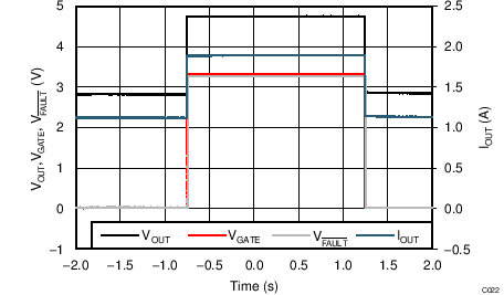
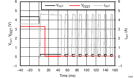
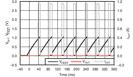
Some applications require that an overcurrent condition disables the part momentarily during a fault condition and re-enables after a pre-set time. This auto-retry functionality can be implemented with an external resistor and capacitor. During a fault condition, FAULT pulls low EN. The part is disabled when EN is pulled below the turn-off threshold, and FAULT goes high impedance allowing C(RETRY) to begin charging. The part re-enables when the voltage on EN reaches the turn-on threshold. The part will continue to cycle in this manner until the fault condition is removed. The auto-retry cycling time is determined by the resistor/capacitor time constant, TPS2559-Q1 turn on time and FAULT deglitch time (see Figure 28).
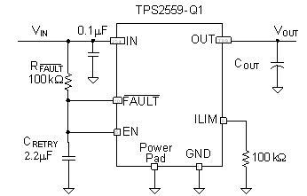 Figure 18. Auto-Retry Circuit
Some applications require auto-retry functionality and the ability to enable/disable with an external logic signal. Figure 19 shows how an external logic signal can drive EN through R(FAULT) and maintain auto-retry functionality. The resistor/capacitor time constant determines the auto-retry time-out period.
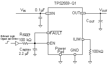 Figure 19. Auto-Retry Circuit with External EN Signal
If need to implement latch-off, refer to application report (SLVA282A).
10.2.2.9 Two-level Current-limit
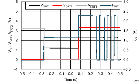
Some applications require different current-limit thresholds depending on external system conditions. Figure 20 shows an implementation for an externally-controlled, two-level current-limit circuit. The current-limit threshold is set by the total resistance from ILIM to GND (see previously discussed Programming the Current-Limit Threshold section). A logic-level input enables/disables MOSFET Q1 and changes the current-limit threshold by modifying the total resistance from ILIM to GND (see Figure 29 and Figure 30). Additional MOSFET/resistor combinations can be used in parallel to Q1/R2 to increase the number of additional current-limit levels.
NOTE
ILIM should never be driven directly with an external signal.
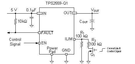 Figure 20. Two-Level Current-Limit Circuit
10.2.3 Application Curves
