SLVSD03 December 2015 TPS2559-Q1
PRODUCTION DATA.
- 1 Features
- 2 Applications
- 3 Description
- 4 Revision History
- 5 Device Comparison Table
- 6 Pin Configuration and Functions
- 7 Specifications
- 8 Parameter Measurement Information
- 9 Detailed Description
-
10Application and Implementation
- 10.1 Application Information
- 10.2
Typical Application
- 10.2.1 Design Requirements
- 10.2.2
Detailed Design Procedure
- 10.2.2.1 Step by Step Design Procedure
- 10.2.2.2 Input and Output Capacitance
- 10.2.2.3 Programming the Current-Limit Threshold
- 10.2.2.4 Design Above a Minimum Current Limit
- 10.2.2.5 Design Below a Maximum Current Limit
- 10.2.2.6 Accounting for Resistor Tolerance
- 10.2.2.7 Power Dissipation and Junction Temperature
- 10.2.2.8 Auto-Retry
- 10.2.2.9 Two-level Current-limit
- 10.2.3 Application Curves
- 11Power Supply Recommendations
- 12Layout
- 13Device and Documentation Support
- 14Mechanical, Packaging, and Orderable Information
Package Options
Refer to the PDF data sheet for device specific package drawings
Mechanical Data (Package|Pins)
- DRC|10
Thermal pad, mechanical data (Package|Pins)
- DRC|10
Orderable Information
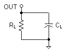
8 Parameter Measurement Information


spacer
spacer

