SLVSDT4F October 2017 – December 2021 TPS2662
PRODUCTION DATA
- 1 Features
- 2 Applications
- 3 Description
- 4 Revision History
- 5 Device Comparison Table
- 6 Pin Configuration and Functions
- 7 Specifications
- 8 Parameter Measurement Information
-
9 Detailed Description
- 9.1 Overview
- 9.2 Functional Block Diagram
- 9.3
Feature Description
- 9.3.1 Undervoltage Lockout (UVLO)
- 9.3.2 Overvoltage Protection (OVP)
- 9.3.3 Hot Plug-In and Inrush Current Control
- 9.3.4 Reverse Polarity Protection
- 9.3.5 Overload and Short-Circuit Protection
- 9.3.6 Reverse Current Protection
- 9.3.7 FAULT Response
- 9.3.8 IN, OUT, RTN, and GND Pins
- 9.3.9 Thermal Shutdown
- 9.4 Device Functional Modes
-
10Application and Implementation
- 10.1 Application Information
- 10.2 Typical Application
- 10.3 System Examples
- 10.4 Do's and Don'ts
- 11Power Supply Recommendations
- 12Layout
- 13Device and Documentation Support
- 14Mechanical, Packaging, and Orderable Information
Package Options
Mechanical Data (Package|Pins)
- DRC|10
Thermal pad, mechanical data (Package|Pins)
- DRC|10
Orderable Information
3 Description
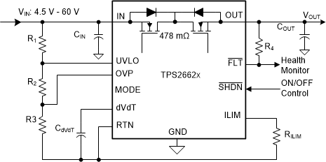
The TPS2662x family are compact, feature rich high voltage eFuses with a full suite of protection features. The wide supply input range of 4.5 V to 60 V allows control of many popular DC bus voltages. The device can withstand and protect the loads from positive and negative supply voltages up to ±60 V. The TPS26624 and TPS26625 devices support both input as well as output reverse polarity protection feature. Integrated back to back FETs provide reverse current blocking feature making the device suitable for systems with output voltage holdup requirements during power fail and brownout conditions. Load, source and device protection are provided with many adjustable features including overcurrent, output slew rate and overvoltage, undervoltage thresholds. The internal robust protection control blocks along with the high voltage rating of the TPS2662x family helps to simplify the system designs for Surge protection.
The TPS26620, TPS26622 and TPS26624 feature latch-off and TPS26621, TPS26623 and TPS26625 feature auto-retry functionality, which are the overtemperature and overcurrent fault events.
The devices are available in a 3 mm × 3 mm 10-pin SON package and are specified over a –40°C to +125°C temperature range.
| PART NUMBER | PACKAGE | BODY SIZE (NOM) |
|---|---|---|
| TPS26620 TPS26621 TPS26622 TPS26623 TPS26624 TPS26625 |
SON (10) | 3.00 mm × 3.00 mm |
 Simplified Schematic
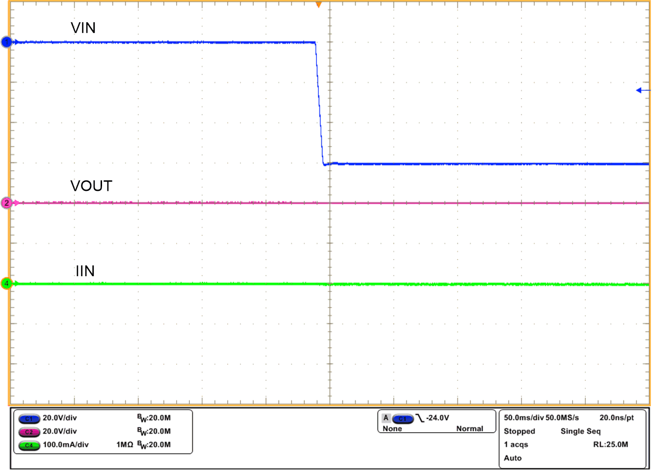
 Reverse Input Polarity Protection at –60-V
Supply