SLVSDZ5A February   2018  – January 2020 TPS2HB50-Q1

PRODUCTION DATA.  

  1. Features
  2. Applications
  3. Description
    1.     Simplified Schematic
  4. Revision History
  5. Device Comparison Table
  6. Pin Configuration and Functions
    1.     Pin Functions
    2. 6.1 Recommended Connections for Unused Pins
  7. Specifications
    1. Table 3. Absolute Maximum Ratings
    2. Table 4. ESD Ratings
    3. Table 5. Recommended Operating Conditions
    4. Table 6. Thermal Information
    5. Table 7. Electrical Characteristics
    6. Table 8. SNS Timing Characteristics
    7. Table 9. Switching Characteristics
    8. 7.1      Typical Characteristics
  8. Parameter Measurement Information
  9. Detailed Description
    1. 9.1 Overview
    2. 9.2 Functional Block Diagram
    3. 9.3 Feature Description
      1. 9.3.1 Protection Mechanisms
        1. 9.3.1.1 Thermal Shutdown
        2. 9.3.1.2 Current Limit
          1. 9.3.1.2.1 Current Limit Foldback
          2. 9.3.1.2.2 Programmable Current Limit
          3. 9.3.1.2.3 Undervoltage Lockout (UVLO)
          4. 9.3.1.2.4 VBB During Short-to-Ground
        3. 9.3.1.3 Voltage Transients
          1. 9.3.1.3.1 Load Dump
        4. 9.3.1.4 Driving Inductive Loads
        5. 9.3.1.5 Reverse Battery
        6. 9.3.1.6 Fault Event – Timing Diagrams
      2. 9.3.2 Diagnostic Mechanisms
        1. 9.3.2.1 VOUTx Short-to-Battery and Open-Load
          1. 9.3.2.1.1 Detection With Switch Enabled
          2. 9.3.2.1.2 Detection With Switch Disabled
        2. 9.3.2.2 SNS Output
          1. 9.3.2.2.1 RSNS Value
            1. 9.3.2.2.1.1 High Accuracy Load Current Sense
            2. 9.3.2.2.1.2 SNS Output Filter
        3. 9.3.2.3 Fault Indication and SNS Mux
        4. 9.3.2.4 Resistor Sharing
        5. 9.3.2.5 High-Frequency, Low Duty-Cycle Current Sensing
    4. 9.4 Device Functional Modes
      1. 9.4.1 Off
      2. 9.4.2 Standby
      3. 9.4.3 Diagnostic
      4. 9.4.4 Standby Delay
      5. 9.4.5 Active
      6. 9.4.6 Fault
  10. 10Application and Implementation
    1. 10.1 Application Information
      1. 10.1.1 Ground Protection Network
      2. 10.1.2 Interface With Microcontroller
      3. 10.1.3 I/O Protection
      4. 10.1.4 Inverse Current
      5. 10.1.5 Loss of GND
      6. 10.1.6 Automotive Standards
        1. 10.1.6.1 ISO7637-2
        2. 10.1.6.2 AEC – Q100-012 Short Circuit Reliability
    2. 10.2 Typical Application
      1. 10.2.1 Design Requirements
      2. 10.2.2 Detailed Design Procedure
        1. 10.2.2.1 Thermal Considerations
        2. 10.2.2.2 RILIM Calculation
        3. 10.2.2.3 Diagnostics
          1. 10.2.2.3.1 Selecting the RSNS Value
      3. 10.2.3 Application Curves
  11. 11Power Supply Recommendations
  12. 12Layout
    1. 12.1 Layout Guidelines
    2. 12.2 Layout Example
  13. 13Device and Documentation Support
    1. 13.1 Documentation Support
      1. 13.1.1 Related Documentation
    2. 13.2 Receiving Notification of Documentation Updates
    3. 13.3 Support Resources
    4. 13.4 Trademarks
    5. 13.5 Electrostatic Discharge Caution
    6. 13.6 Glossary
  14. 14Mechanical, Packaging, and Orderable Information

Package Options

Mechanical Data (Package|Pins)
Thermal pad, mechanical data (Package|Pins)
Orderable Information

Application Curves

When the device receives a rising edge on the ENx pulse the output will turn on as shown in . After the turn-on delay time, the device VOUT goes to the VBB supply and begins outputting the steady state resistive current.
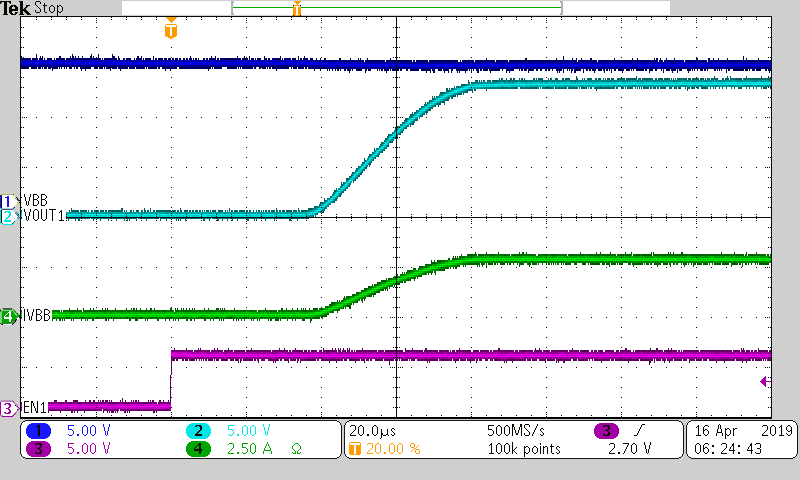
TPS2HB50-Q1 TPS2HB50B_turnon - 4 channel.pngFigure 47. Turn On Waveform

When the device turns off on a falling edge of ENx, the channel IOUT will go to zero and the VOUT will drop to zero as well as shown in Figure 48.
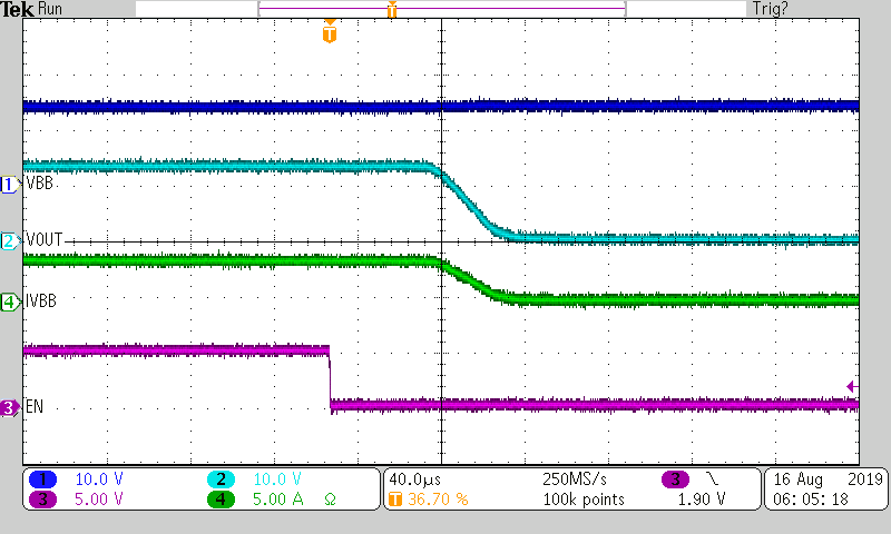
TPS2HB50-Q1 ss2.pngFigure 48. Turn-Off Waveform

While enabled, it is important to measure the output current through both channels. Figure 49 shows this behavior when toggling the SELx pins. The image shows that when SEL2 toggles high to low, the SNS pin toggles between representing IOUT1 and IOUT2. When SEL2 is low SNS represents IOUT1 and when SEL2 is high SNS represents IOUT2. This image shows that channel 2 is currently outputting twice the output current as channel 1.
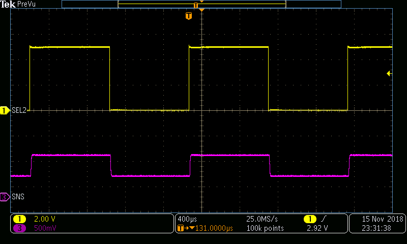
TPS2HB50-Q1 SNS Change Channel.pngFigure 49. Toggling Between CH1 and CH2 Current Measurement
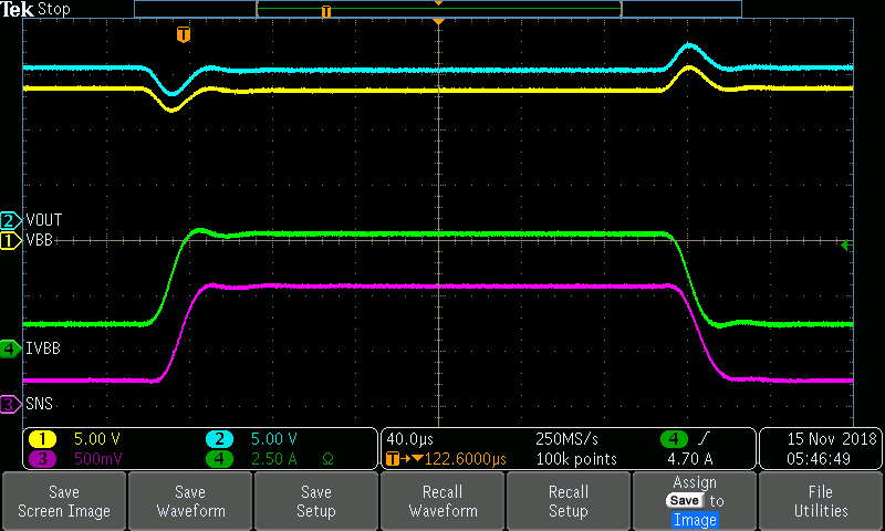
TPS2HB50-Q1 Load Step Settling.pngFigure 50. SNS Settling Time

If the output of the TPS2HB50-Q1 is short-circuited, the device will protect the system from failure. shows the device turning off the output at a set current limit when the output is short circuited. (Note: Figure 51shows a case with a higher RILIM than calculated in this example, so the current limit is higher than 18 A).
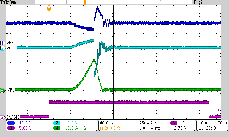
TPS2HB50-Q1 TPS2HB50B_STGB__VBB=13p5__TEMP=25.pngFigure 51. TPS2HB50B-Q1 Short Circuit Waveform