SNVSB67A July   2018  – October 2021 TPS3431-Q1

PRODUCTION DATA  

  1. Features
  2. Applications
  3. Description
  4. Revision History
  5. Pin Configuration and Functions
  6. Specifications
    1. 6.1 Absolute Maximum Ratings
    2. 6.2 ESD Ratings
    3. 6.3 Recommended Operating Conditions
    4. 6.4 Thermal Information
    5. 6.5 Electrical Characteristics
    6. 6.6 Timing Requirements
    7. 6.7 Timing Diagrams
    8. 6.8 Typical Characteristics
  7. Detailed Description
    1. 7.1 Overview
    2. 7.2 Functional Block Diagram
    3. 7.3 Feature Description
      1. 7.3.1 Enable Input (EN) and Enable Output (ENOUT)
      2. 7.3.2 Watchdog Mode
        1. 7.3.2.1 CWD
        2. 7.3.2.2 Watchdog Input WDI
        3. 7.3.2.3 Watchdog Output WDO
        4. 7.3.2.4 SET1
    4. 7.4 Device Functional Modes
      1. 7.4.1 VDD is Below VPOR ( VDD < VPOR)
      2. 7.4.2 Above Power-On-Reset, But Less Than VDD(min) (VPOR ≤ VDD < VDD(min))
      3. 7.4.3 Normal Operation (VDD ≥ VDD(min))
  8. Application and Implementation
    1. 8.1 Application Information
      1. 8.1.1 CWD Functionality
        1. 8.1.1.1 Factory-Programmed Timing Options
        2. 8.1.1.2 CWD Adjustable Capacitor Watchdog Timeout
    2. 8.2 Typical Application
      1. 8.2.1 Design 1 Requirements
      2. 8.2.2 Detailed Design 1 Procedure
        1. 8.2.2.1 Calculating WDO Pullup Resistor Design 1
        2. 8.2.2.2 Setting the Watchdog Design 1
      3. 8.2.3 Application Curves Design 1
    3. 8.3 Programmable Application
      1. 8.3.1 Design 2 Requirements
      2. 8.3.2 Detailed Design 2 Procedure
        1. 8.3.2.1 Calculating WDO Pullup Resistor Design 2
        2. 8.3.2.2 Setting the Watchdog Design 2
        3. 8.3.2.3 Watchdog Disabled During Initialization Period Design 2
        4. 8.3.2.4 Programmable Disable Feature Design 2
      3. 8.3.3 Application Curves Design 2
  9. Power Supply Recommendations
  10. 10Layout
    1. 10.1 Layout Guidelines
    2. 10.2 Layout Example
  11. 11Device and Documentation Support
    1. 11.1 Device Support
    2. 11.2 Documentation Support
      1. 11.2.1 Related Documentation
    3. 11.3 Receiving Notification of Documentation Updates
    4. 11.4 Support Resources
    5. 11.5 Trademarks
    6. 11.6 Electrostatic Discharge Caution
    7. 11.7 Glossary
  12. 12Mechanical, Packaging, and Orderable Information

Package Options

Mechanical Data (Package|Pins)
Thermal pad, mechanical data (Package|Pins)
Orderable Information

SET1

The SET1 pin can enable and disable the watchdog timer and should be used when disabling the watchdog timer for longer than one watchdog reset cycle. If SET1 is set to GND, the watchdog timer is disabled and WDI is ignored. If the watchdog timer is disabled, drive the WDI pin to either GND or VDD to ensure that there is no increase in IDD. When SET1 is logic high, the watchdog operates normally. The SET1 pin can be changed dynamically; however, if the watchdog is going from disabled to enabled there is a 150 µs setup time where the watchdog does not respond to changes on WDI, as shown in Figure 7-2. Note: disabling using SET1 pin causes a delay defined by the fixed 150-us setup time when enabling again.
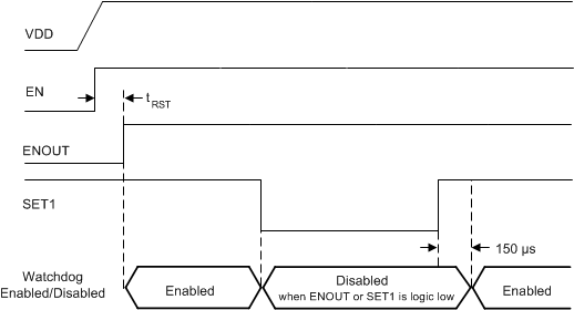
GUID-3638A12B-78BD-47B4-AD08-AC5BD30D2261-low.gifFigure 7-2 Enabling and Disabling the Watchdog