SBVS231A August 2014 – March 2015 TPS3847
PRODUCTION DATA.
- 1 Features
- 2 Applications
- 3 Description
- 4 Revision History
- 5 Pin Configuration and Functions
- 6 Specifications
- 7 Detailed Description
- 8 Application and Implementation
- 9 Power Supply Recommendations
- 10Layout
- 11Device and Documentation Support
- 12Mechanical, Packaging, and Orderable Information
Package Options
Mechanical Data (Package|Pins)
- DBV|5
Thermal pad, mechanical data (Package|Pins)
Orderable Information
7 Detailed Description
7.1 Overview
The TPS3847 is a family of ultralow-current supervisors for high-voltage applications that are specified from –40°C to +85°C and operational up to 105°C (see the Typical Characteristics section for typical –40°C to +105°C performance).
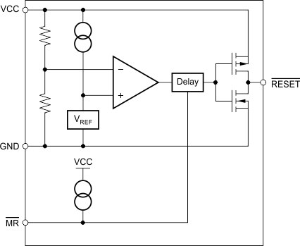
The RESET output goes low after the power-supply voltage (V(VCC)) drops below the negative-going input threshold voltage (VIT–), and after the VCC falling propagation delay (tpd(VCC)) elapses. When V(VCC) rises above the positive-going reset threshold (VIT+), which is the negative-going threshold voltage plus the hysteresis (VIT– + Vhys), RESET outputs a high signal after the reset delay time (td) elapses.
The TPS3847 also features a manual reset pin (MR) that allows a processor, or other logic devices, to initiate a reset, even when V(VCC) exceeds VIT–. A logic low on MR causes RESET to transition to logic low after the MR propagation delay (tpd(MR)) elapses. When MR returns to a logic high and V(VCC) exceeds VIT+, RESET transitions to logic high after td elapses.
7.2 Functional Block Diagram
7.3 Feature Description
7.3.1 Ultralow Supply Current
The TPS3847 uses a unique sampling scheme to maintain an extremely-low average quiescent current of
380 nA. This low quiescent current is ideal for applications that require extremely-low power consumption.
7.3.2 Wide Supply Range
This device has an operational input supply range of 4.5 V to 18 V, allowing for a wide range of applications. This wide supply range is ideal for applications that have either large transients or high dc voltage supplies.
7.3.3 High-Accuracy Negative Threshold
The TPS3847 has a negative threshold accuracy of ±2.5% and uses well-controlled and matched internal resistors to set the threshold voltage in order to eliminate the inaccuracies because of the external resistors. Unlike The TPS3847, voltage supervisors that require external resistors to set the threshold voltage always add inaccuracy to the specified performance.
7.3.4 Push-Pull Output
The TPS3847 has a push-pull output stage that covers many of the common digital logic levels. Push-pull outputs simplify many designs compared to open-drain output devices because push-pull outputs do not require a pull-up resistor or an additional low-voltage rail. Compared to open-drain output devices, push-pull devices reduce power consumption when the output is low because open-drain devices sink current through the pull-up resistor to ground in order to create the logic-low signal.
7.3.5 Manual Reset (MR) Input
The manual reset (MR) input allows a processor, or other logic devices, to initiate a reset even when the voltage on VCC is greater than VIT–. A logic low on MR causes RESET to output a logic low. After MR returns to a logic high and the power-supply voltage is greater than VIT+, RESET transitions to logic high after the reset delay time (td) elapses.
7.3.6 VCC Transient Rejection
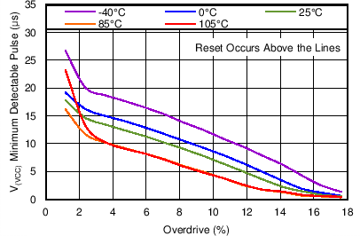
The TPS3847 has built-in rejection of fast transients on the VCC pin. Transient rejection depends on both the duration and overdrive, or amplitude, of the transient. Overdrive of the transient is measured from the bottom of the transient to the negative threshold voltage (VIT–) of the device, as shown in Figure 11.
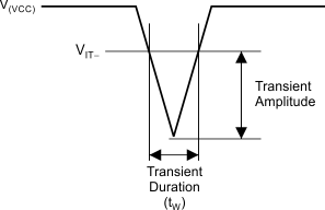 Figure 11. Voltage Transient Measurement
Figure 12 shows the relationship between the overdrive and the duration required to trigger a reset. Any combination of duration and amplitude greater than that shown in Figure 12 generates a reset signal.
7.3.7 Controlled Startup Current
The input supply current of the TPS3847 is very well controlled, including during startup. Some low-current devices exhibit spikes in the supply current before reaching the minimum supply voltage; this type of startup behavior can cause problems in some applications. Figure 13 shows that there are no spikes in supply current, and the device is well controlled all the way from 0 V to minimum V(VCC).
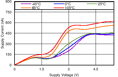 Figure 13. Supply Current During Startup
7.3.8 Low Minimum Supply Voltage for Valid Output
The TPS3847 is designed to have a valid RESET signal, even with a low input supply voltage. Figure 14 shows that even at –40°C, the TPS3847 typically has a valid output with only 0.65 V on the input supply; at 105°C, that input supply voltage goes down to less than 0.45 V.
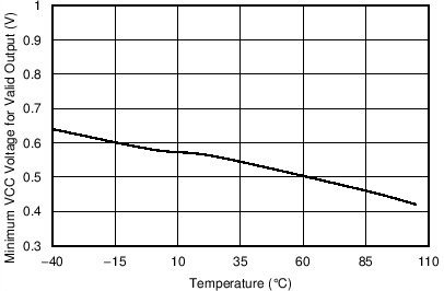 Figure 14. Minimum Supply Voltage for Valid Output vs Temperature
7.4 Device Functional Modes
The TPS3847 has two functional modes:
- MR high: in this mode, RESET is high or low depending on the value of V(VCC) relative to VIT–.
- MR low: in this mode, RESET is held low regardless of the value of V(VCC).
