SBVS231A August 2014 – March 2015 TPS3847
PRODUCTION DATA.
- 1 Features
- 2 Applications
- 3 Description
- 4 Revision History
- 5 Pin Configuration and Functions
- 6 Specifications
- 7 Detailed Description
- 8 Application and Implementation
- 9 Power Supply Recommendations
- 10Layout
- 11Device and Documentation Support
- 12Mechanical, Packaging, and Orderable Information
Package Options
Mechanical Data (Package|Pins)
- DBV|5
Thermal pad, mechanical data (Package|Pins)
Orderable Information
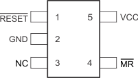
5 Pin Configuration and Functions
DBV Package
5-Pin SOT
(Top View)

Pin Functions
| PIN | I/O | DESCRIPTION | |
|---|---|---|---|
| NAME | NO. | ||
| GND | 2 | — | Ground |
| MR | 4 | I | Manual reset. Pull this pin to a logic low to force the RESET output low regardless of the voltage on VCC. After the MR pin is pulled to a logic high, the RESET output goes high after the RESET delay time (td) if the voltage on VCC is higher than the positive-going threshold voltage. |
| NC | 3 | — | No internal connection. |
| RESET | 1 | O | Active low reset output. RESET stays low as long as the voltage on VCC is below the factory trimmed threshold voltage. RESET transitions from low to high once the VCC voltage is above the positive-going threshold voltage for a specified time (td). RESET is a push-pull output. |
| VCC | 5 | I | Power supply and monitored voltage. TI recommends adding a small 0.1-μF bypass capacitor near the VCC pin. |