SBVS172B July 2011 – April 2015
PRODUCTION DATA.
- 1 Features
- 2 Applications
- 3 Description
- 4 Revision History
- 5 Device Comparison Table
- 6 Pin Configuration and Functions
- 7 Specifications
- 8 Detailed Description
- 9 Applications and Implementation
- 10Power Supply Recommendations
- 11Layout
- 12Device and Documentation Support
- 13Mechanical, Packaging, and Orderable Information
Package Options
Mechanical Data (Package|Pins)
- DRY|6
Thermal pad, mechanical data (Package|Pins)
- DRY|6
Orderable Information
9 Applications and Implementation
NOTE
Information in the following applications sections is not part of the TI component specification, and TI does not warrant its accuracy or completeness. TI’s customers are responsible for determining suitability of components for their purposes. Customers should validate and test their design implementation to confirm system functionality.
9.1 Application Information
The TPS389x family of devices are very small supervisory circuits that monitor voltages greater than 500 mV and offer an adjustable delay time using external capacitors. The TPS389x family operates from 1.7 V to 6.5 V and also has an enable pin to power on/off the output. Orderable options include versions with either push-pull or open-drain outputs as well as versions that use active-high or active-low logic for the output and enable signals.
9.2 Typical Applications
9.2.1 Single-Rail Monitoring
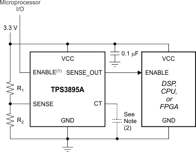
The TPS3895P can be used to monitor the supply rail for devices such as digital signal processors (DSPs), central processing units (CPUs), or field-programmable gate arrays (FPGAs). The downstream device is enabled by the TPS3895P once the voltage on the SENSE pin (VSENSE) is above the threshold voltage (VIT+) set by the resistor divider. The downstream device is disabled by the TPS3895P when VSENSE is falls below the threshold voltage minus the hysteresis voltage (VIT+ – Vhys).
If active low inputs or outputs are needed, replace the TPS3895P devices with TPS3896P devices. Figure 23 shows the TPS3895P in a typical application.
9.2.1.1 Design Requirements
The TPS3895P must drive the enable pin of devices using a logic-high signal to signify that the supply voltage is above the minimum operating voltage of the device.
9.2.1.2 Detailed Design Procedure
Select R1 and R2 so the voltage at SENSE (VSENSE) is above the positive-going threshold voltage (VIT+) at the supply voltage required for proper device operation (that is, proper operation of the DSP, CPU, FPGA, and so on). Also, ensure that the current that flows from the supply voltage to ground through the resistor divider is at least 100 times larger than the input current (ISENSE).
If an output delay time is required, connect a capacitor from CT to GND; see the Output Delay Time Pin (CT) section for more information. If no CT cap is connected, the delay time is 40 µs.
9.2.1.3 Application Curve
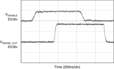 Figure 24. Enable Power On and Power Off Delay (TPS3895P)
9.2.2 Multiple Voltage Monitoring Sequential Delay
Multiple TPS3895As can be used to monitor multiple supply rails with a single output signifying whether or not all rails are above the respective thresholds. Some applications may need a minimum total delay time that is the sum of all the delay times of the supply monitor. To achieve this configuration, connect the output of one TPS3895A to the ENABLE pin of the next TPS3895A, and repeat until the last TPS3895A is connected to the device that receives the final Wired-AND signal. The downstream device receives a signal from the last TPS3895A once VSENSE on all SENSE pins is above the VIT+ set by the resistor dividers. The downstream device is disabled by the last TPS3895A if the voltage on any SENSE pin in the chain falls below (VIT+ – Vhys).
Figure 25 shows an example of a configuration for dual-supply monitoring; this concept can be expanded for as many rails as a given application requires.
If active low inputs or outputs are needed, replace the TPS3895A devices with TPS3896A devices.
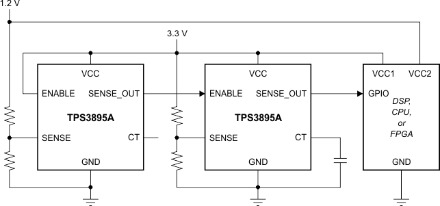 Figure 25. Multiple Voltage Monitoring Using ENABLE Pin
9.2.2.1 Design Requirements
Two rails must be monitored to ensure that both are above the respective minimum operating voltage for proper operation pf the device. The TPS3895As must drive a GPIO pin of the final downstream device, and use a logic-high signal to signify that the supply voltages are above the minimum operating voltage of the given device.
9.2.2.2 Detailed Design Procedure
Select the resistor divider of each TPS3895A so the voltage at SENSE (VSENSE) is above the positive-going threshold voltage (VIT+) at the point where the monitored voltage is required for proper device operation (that is, proper operation of the DSP, CPU, FPGA, and so on). Also, ensure that the currents that flow from the monitored voltage to ground through the resistor dividers are at least 100 times larger than the input current (ISENSE).
If an output delay time is required for any of the TPS3895As, connect a capacitor from the CT pin of that TPS3895A to GND; see the Output Delay Time Pin (CT) section for more information. If no CT caps are connected, the delay time is 40 µs for each TPS3895A in the chain. Because each of the ENABLE pins is tied to the TPS3895A preceding it (other than the first), at a minimum the total delay time is the sum of all the delay times set by the CT pins in the design.
9.2.2.3 Application Curve
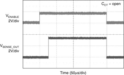 Figure 26. Enable Power On and Power Off Delay (TPS3895A)
9.2.3 Multiple Voltage Monitoring Minimum Delay
Multiple TPS3897Ps can be used to monitor multiple supply rails with a single output that signals if all rails are above the respective thresholds. Some applications may need a minimum total delay time that is equal to the delay time of only the final supply monitor to power up. To achieve this configuration, connect the outputs of all the TPS3897Ps to the device that must receive the final Wired-AND signal and connect that same node to the appropriate logic-high voltage via a resistor. The downstream device receives a signal once VSENSE on all SENSE pins are above the VIT+ set by the resistor dividers. The downstream device is disabled if the voltage on any SENSE pin falls below (VIT+ – Vhys).
See Figure 27 for an example of a configuration for dual-supply monitoring. This concept can be expanded for as many rails as a given application requires.
If active low inputs/outputs are required, replace the TPS3897P devices with TPS3898P devices.
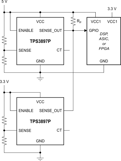 Figure 27. Multiple Voltage Monitoring Using Wired-OR Logic at SENSE_OUT
9.2.3.1 Design Requirements
Two rails must be monitored to ensure that both rails are above the respective minimum operating voltage for proper operation of the device. The TPS3897Ps must drive a GPIO pin of the final downstream device and use a logic-high signal to signify that the supply voltages are above the minimum operating voltage of the device.
9.2.3.2 Detailed Design Procedure
Select the resistor divider of each TPS3897P so the voltage at SENSE (VSENSE) is above the positive-going threshold voltage (VIT+) at the point where the monitored voltage is required for proper device operation (that is, proper operation of the DSP, CPU, FPGA, and so on). Also, ensure that the currents that flow from the monitored voltage to ground through the resistor dividers are at least 100 times larger than the input current (ISENSE).
If an output delay time is required for any of the TPS3897Ps, connect a capacitor from the CT pin of that TPS3897P to GND; see the Output Delay Time Pin (CT) section for more information. If no CT caps are connected, the delay time is 40 µs.
Determine the logic-high voltage by selecting the voltage that the pullup resistor (denoted RP in Figure 29) is connected to. Select RP so that current that flows to ground allows for a low-level output voltage that is low enough for the specific application. See the Output Pin (SENSE_OUT) section for more information.
9.2.3.3 Application Curves
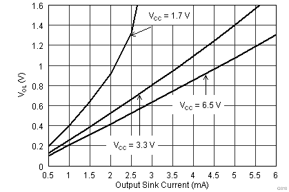 Figure 28. Output Voltage Low vs Output Current
9.2.4 Voltage Sequencing
TPS3895As can be used to implement voltage rail sequencing by connecting a resistor divider and the SENSE pin of a TPS3895A to the first rail to be monitored, and then feeding the output from the first TPS3895A to the ENABLE pin of the next voltage rail. The downstream voltage rail is enabled by the TPS3895A once the voltage on the SENSE pin (VSENSE) is above the threshold voltage (VIT+) set by the resistor divider. This process can be repeated for as many rails as the application requires. The downstream voltage rail is disabled by the TPS3895A when VSENSE falls below the threshold voltage minus the hysteresis voltage (VIT+ – Vhys).
If active low inputs/outputs are required, replace the TPS3895A devices with TPS3896A devices.
See Figure 29 for an example for a system with four voltage rails that must sequence the three LDOs.
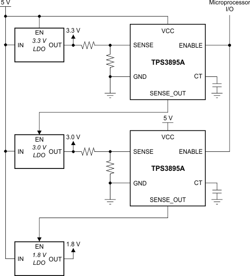 Figure 29. Voltage Sequencing (5 V → 3.3 V → 3 V → 1.8 V)
9.2.4.1 Design Requirements
Three rails must be sequenced to ensure proper start-up sequencing. The TPS3895As must drive the ENABLE pins of each LDO, and use a logic-high signal to signify that the supply preceding it is above the desired operating voltage for that rail. The ENABLE pin of the TPS3895As must be controlled by a microprocessor to allow it to be shut down even when the rails are above the threshold.
9.2.4.2 Detailed Design Procedure
Select the resistor divider of each TPS3895A so the voltage at SENSE (VSENSE) is above the positive-going threshold voltage (VIT+) at the point where the monitored voltage is required for proper device operation (that is, proper operation of the DSP, CPU, FPGA, and so on). Also, ensure that the currents that flow from the monitored voltage to ground through the resistor dividers are at least 100 times larger than the input current (ISENSE).
If an output delay time is required for any of the TPS3895As, connect a capacitor from the CT pin of that TPS3895A to GND; see the Output Delay Time Pin (CT) section for more information. If no CT caps are connected, the delay time is 40 µs for each TPS3895A in the chain. Because each of the ENABLE pins is tied to the TPS3895A that precedes it (other than the first device in the chain), at a minimum the total delay time is the sum of all the delay times set by the CT pins.
9.2.4.3 Application Curve
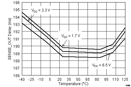 Figure 30. SENSE_OUT Time-out Period vs Temperature (CCT = 47 nF)