SLVS861F august 2008 – june 2020 TPS40210-Q1 , TPS40211-Q1
PRODUCTION DATA
- 1 Features
- 2 Applications
- 3 Description
- 4 Revision History
- 5 Pin Configuration and Functions
- 6 Specifications
-
7 Detailed Description
- 7.1 Overview
- 7.2 Functional Block Diagram
- 7.3
Feature Description
- 7.3.1 Minimum On-Time and Off-Time Considerations
- 7.3.2 Current Sense and Overcurrent
- 7.3.3 Current Sense and Subharmonic Instability
- 7.3.4 Current Sense Filtering
- 7.3.5 Soft Start
- 7.3.6 BP Regulator
- 7.3.7 Shutdown (DIS/ EN Pin)
- 7.3.8 Control Loop Considerations
- 7.3.9 Gate Drive Circuit
- 7.3.10 TPS40211-Q1
- 7.4 Device Functional Modes
-
8 Application and Implementation
- 8.1 Application Information
- 8.2
Typical Application
- 8.2.1 Design Requirements
- 8.2.2
Detailed Design Procedure
- 8.2.2.1 Duty Cycle Estimation
- 8.2.2.2 Inductor Selection
- 8.2.2.3 Rectifier Diode Selection
- 8.2.2.4 Output Capacitor Selection
- 8.2.2.5 Input Capacitor Selection
- 8.2.2.6 Current Sense and Current Limit
- 8.2.2.7 Current Sense Filter
- 8.2.2.8 Switching MOSFET Selection
- 8.2.2.9 Feedback Divider Resistors
- 8.2.2.10 Error Amplifier Compensation
- 8.2.2.11 R-C Oscillator
- 8.2.2.12 Soft-Start Capacitor
- 8.2.2.13 Regulator Bypass
- 8.2.3 Application Curves
- 9 Power Supply Recommendations
- 10Layout
- 11Device and Documentation Support
- 12Mechanical, Packaging, and Orderable Information
Package Options
Refer to the PDF data sheet for device specific package drawings
Mechanical Data (Package|Pins)
- DGQ|10
Thermal pad, mechanical data (Package|Pins)
Orderable Information
7.3.8 Control Loop Considerations
There are two methods to design a suitable control loop for the TPS4021x device. The first (and preferred, if equipment is available) is to use a frequency-response analyzer to measure the open-loop modulator and power stage gain and to then design compensation to fit that. The usage of these tools for this purpose is well-documented with the literature that accompanies the tool and is not discussed here.
The second option is to make an initial guess at compensation, and then evaluate the transient response of the system to see if the compensation is acceptable to the application or not. For most systems, an adequate response can be obtained by simply placing a series resistor and capacitor (RFB and CFB) from the COMP pin to the FB pin as shown in Figure 7-6.
 Figure 7-6 Basic Compensation Network
The natural phase characteristics of most capacitors used for boost outputs combined with the current mode control provide adequate phase margin when using this type of compensation. To determine an initial starting point for the compensation, the desired crossover frequency must be considered when estimating the control to output gain. The model used is a current source into the output capacitor and load.
When using these equations, the loop bandwidth should be no more than 20% of the switching frequency, fSW. A more reasonable loop bandwidth would be 10% of the switching frequency. Be sure to evaluate the transient response of the converter over the expected load range to ensure acceptable operation.

where
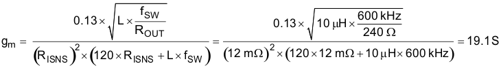
- KCO is the control to output gain of the converter, in V/V
- gM is the transconductance of the power stage and modulator, in S
- ROUT is the output load equivalent resistance, in Ω
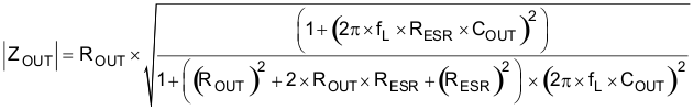
- ZOUT is the output impedance, including the output capacitor, in Ω
- RISNS is the value of the current sense resistor, in Ω
- L is the value of the inductor, in H
- COUT is the value of the output capacitance, in μF
- RESR is the equivalent series resistance of COUT, in Ω
- fSW is the switching frequency, in Hz
- fL is the desired crossover frequency for the control loop, in Hz
These equations assume that the operation is discontinuous and that the load is purely resistive. The gain in continuous conduction can be found by evaluating Equation 22 at the resistance that gives the critical conduction current for the converter. Loads that are more like current sources give slightly higher gains than predicted here. To find the gain of the compensation network required for a control loop of bandwidth fL, take the reciprocal of Equation 21.
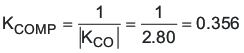
The GBWP of the error amplifier is only specified to be at least 1.5 MHz. If KCOMP multiplied by the fL is greater than 750 kHz, reduce the desired loop crossover frequency until this condition is satisfied. This ensures that the high-frequency pole from the error amplifier response with the compensation network in place does not cause excessive phase lag at the fL and decrease phase margin in the loop.
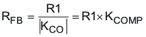
The R-C network connected from COMP to FB places a zero in the compensation response. That zero should be approximately 1/10th of the desired crossover frequency, fL. With that being the case, RFB and CFB can be found from Equation 25 and Equation 26.
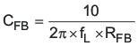
where
- R1 is in fL is the loop crossover frequency desired, in Hz
- RFB is the feedback resistor in CFB is the feedback capacitance in μF
Though not strictly necessary, it is recommended that a capacitor be added between COMP and FB to provide high-frequency noise attenuation in the control loop circuit. This capacitor introduces another pole in the compensation response. The allowable location of that pole frequency determines the capacitor value. As a starting point, the pole frequency should be 10 × fL. The value of CHF can be found from Equation 27.
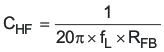
The error amplifier GBWP will usually be higher, but is ensured by design to be at least 1.5 MHz. If the gain required in Equation 24 multiplied by 10 times the desired control loop crossover frequency, the high-frequency pole introduced by CHF is overridden by the error amplifier capability and the effective pole is lower in frequency. If this is the case, CHF can be made larger to provide a consistent high-frequency roll off in the control loop design. Equation 28 calculates the required CHF in this case.
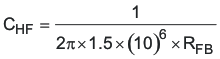
where
- CHF is the high-frequency roll-off capacitor value in μF
- RFB is the mid-band gain-setting resistor value in Ω