SLUSBO6C JANUARY 2014 – October 2018 TPS40425
PRODUCTION DATA.
- 1 Features
- 2 Applications
- 3 Description
- 4 Revision History
- 5 Pin Configuration and Functions
- 6 Specifications
-
7 Detailed Description
- 7.1 Overview
- 7.2 Functional Block Diagram
- 7.3
Feature Description
- 7.3.1 Asynchronous Pulse Injection (API)
- 7.3.2 Adaptive Voltage Scaling (AVS)
- 7.3.3 Switching Frequency and Synchronization
- 7.3.4 Voltage Reference
- 7.3.5 Output Voltage and Remote Sensing Amplifier
- 7.3.6 Current Sensing and Temperature Sensing Modes
- 7.3.7 Current Sensing
- 7.3.8 Temperature Sensing
- 7.3.9 Current Sharing
- 7.3.10 Linear Regulators
- 7.3.11 Power Sequence Between TPS40425 Device and Power Stage
- 7.3.12 PWM Signal
- 7.3.13 Startup and Shutdown
- 7.3.14 Pre-Biased Output Start-up
- 7.3.15 PGOOD Indication
- 7.3.16 Overcurrent Protection
- 7.3.17 Overvoltage/Undervoltage Protection
- 7.3.18 Overtemperature Fault Protection
- 7.3.19 Input Undervoltage Lockout (UVLO)
- 7.3.20 Fault Communication
- 7.3.21 Fault Protection Summary
- 7.4 Device Functional Modes
- 7.5 Programming
- 7.6 Register Maps
- 7.7
Supported PMBus Commands
- 7.7.1 PAGE (00h)
- 7.7.2 OPERATION (01h)
- 7.7.3 ON_OFF_CONFIG (02h)
- 7.7.4 CLEAR_FAULTS (03h)
- 7.7.5 WRITE_PROTECT (10h)
- 7.7.6 STORE_USER_ALL (15h)
- 7.7.7 RESTORE_USER_ALL (16h)
- 7.7.8 CAPABILITY (19h)
- 7.7.9 VOUT_MODE (20h)
- 7.7.10 VIN_ON (35h)
- 7.7.11 VIN_OFF (36h)
- 7.7.12 IOUT_CAL_GAIN (38h)
- 7.7.13 IOUT_CAL_OFFSET (39h)
- 7.7.14 IOUT_OC_FAULT_LIMIT (46h)
- 7.7.15 IOUT_OC_FAULT_RESPONSE (47h)
- 7.7.16 IOUT_OC_WARN_LIMIT (4Ah)
- 7.7.17 OT_FAULT_LIMIT (4Fh)
- 7.7.18 OT_WARN_LIMIT (51h)
- 7.7.19 TON_RISE (61h)
- 7.7.20 STATUS_BYTE (78h)
- 7.7.21 STATUS_WORD (79h)
- 7.7.22 STATUS_VOUT (7Ah)
- 7.7.23 STATUS_IOUT (7Bh)
- 7.7.24 STATUS_TEMPERATURE (7Dh)
- 7.7.25 STATUS_CML (7Eh)
- 7.7.26 STATUS_MFR_SPECIFIC (80h)
- 7.7.27 READ_VOUT (8Bh)
- 7.7.28 READ_IOUT (8Ch)
- 7.7.29 READ_TEMPERATURE_2 (8Eh)
- 7.7.30 PMBus_REVISION (98h)
- 7.7.31 MFR_SPECIFIC_00 (D0h)
- 7.7.32 MFR_SPECIFIC_04 (VREF_TRIM) (D4h)
- 7.7.33 MFR_SPECIFIC_05 (STEP_VREF_MARGIN_HIGH) (D5h)
- 7.7.34 MFR_SPECIFIC_06 (STEP_VREF_MARGIN_LOW) (D6h)
- 7.7.35 MFR_SPECIFIC_07 (PCT_VOUT_FAULT_PG_LIMIT) (D7h)
- 7.7.36 MFR_SPECIFIC_08 (SEQUENCE_TON_TOFF_DELAY) (D8h)
- 7.7.37 MFR_SPECIFIC_16 (COMM_EEPROM_SPARE) (E0h)
- 7.7.38 MFR_SPECIFIC_21 (OPTIONS) (E5h)
- 7.7.39 MFR_SPECIFIC_22 (PWM_OSC_SELECT) (E6h)
- 7.7.40 MFR_SPECIFIC_23 (MASK SMBALERT) (E7h)
- 7.7.41 MFR_SPECIFIC_25 (AVS_CONFIG) (E9h)
- 7.7.42 MFR_SPECIFIC_26 (AVS_ADDRESS) (EAh)
- 7.7.43 MFR_SPECIFIC_27 (AVS_DAC_DEFAULT) (EBh)
- 7.7.44 MFR_SPECIFIC_28 (AVS_CLAMP_HI) (ECh)
- 7.7.45 MFR_SPECIFIC_29 (AVS_CLAMP_LO) (EDh)
- 7.7.46 MFR_SPECIFIC_30 (TEMP_OFFSET) (EEh)
- 7.7.47 MFR_SPECIFIC_32 (API_OPTIONS) (F0h)
- 7.7.48 MFR_SPECIFIC_44 (DEVICE_CODE) (FCh)
-
8 Applications and Implementation
- 8.1 Application Information
- 8.2
Typical Application
- 8.2.1 Dual-Output Application
- 8.2.2 Design Requirements
- 8.2.3
Design Procedure
- 8.2.3.1 Switching Frequency Selection
- 8.2.3.2 Inductor Selection
- 8.2.3.3 Output Capacitor Selection
- 8.2.3.4 Input Capacitor Selection
- 8.2.3.5 VDD, BP5, BP3 Bypass Capacitor
- 8.2.3.6 R-C Snubber
- 8.2.3.7 Current and Temperature Sensor
- 8.2.3.8 Power Sequence Between the TPS40425 Device and Power Stage
- 8.2.3.9 Output Voltage Setting and Frequency Compensation Selection
- 8.2.3.10 Key PMBus Parameter Selection
- 8.2.4 Application Curves
- 9 Power Supply Recommendations
- 10Layout
- 11Device and Documentation Support
- 12Mechanical, Packaging, and Orderable Information
Package Options
Mechanical Data (Package|Pins)
- RHA|40
Thermal pad, mechanical data (Package|Pins)
- RHA|40
Orderable Information
7.3.8 Temperature Sensing
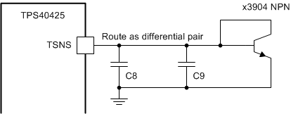
As shown in Figure 15, the non smart-power operation is selected and ΔVbe measurement of external diode (x3904) is used for temperature sensing. The external diode must be placed close to the inductor if the inductor DCR is used for current sensing, so that the current readout can be more accurate with temperature compensation. It is recommended to place a 1-nF capacitor between the TSNS pin and AGND, and another 1-nF bypass capacitor for the transistor. A separate AGND trace is recommended for the TSNS signal. Route the TSNS trace and the AGND trace as a differential pair.
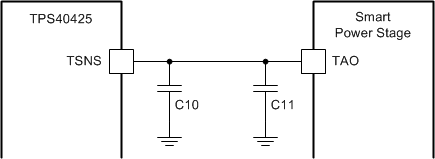
For temperature sensing using a smart-power stage as shown in Figure 16, the smart-power operation is selected for temperature sensing. Local bypass capacitors are recommended for the TSNS pin of the TPS40425 device and the TAO pin of the smart power stage. The total capacitance of the two bypass capacitors should not exceed 1 nF. The recommended value for both C10 and C11 is 470 pF.
In all cases, the temperature sense trace must be placed in a quiet area and be as short as possible.
NOTE
When the device is operating in non-smart power mode, the temperature sensing must be based on the Vbe measurement of the external diode. The TAO signal of power stage can not be used for temperature sensing.
When the device is operating in smart-power mode, the temperature sensing must be based on the TAO signal of power stage.
 Figure 15. Temperature Sensing Using External Diode
  Figure 16. Temperature Sensing Using Smart-Power Stage