SLVSA82F March 2011 – December 2014 TPS43330-Q1 , TPS43332-Q1
PRODUCTION DATA.
- 1 Features
- 2 Applications
- 3 Description
- 4 Revision History
- 5 Device Comparison Table
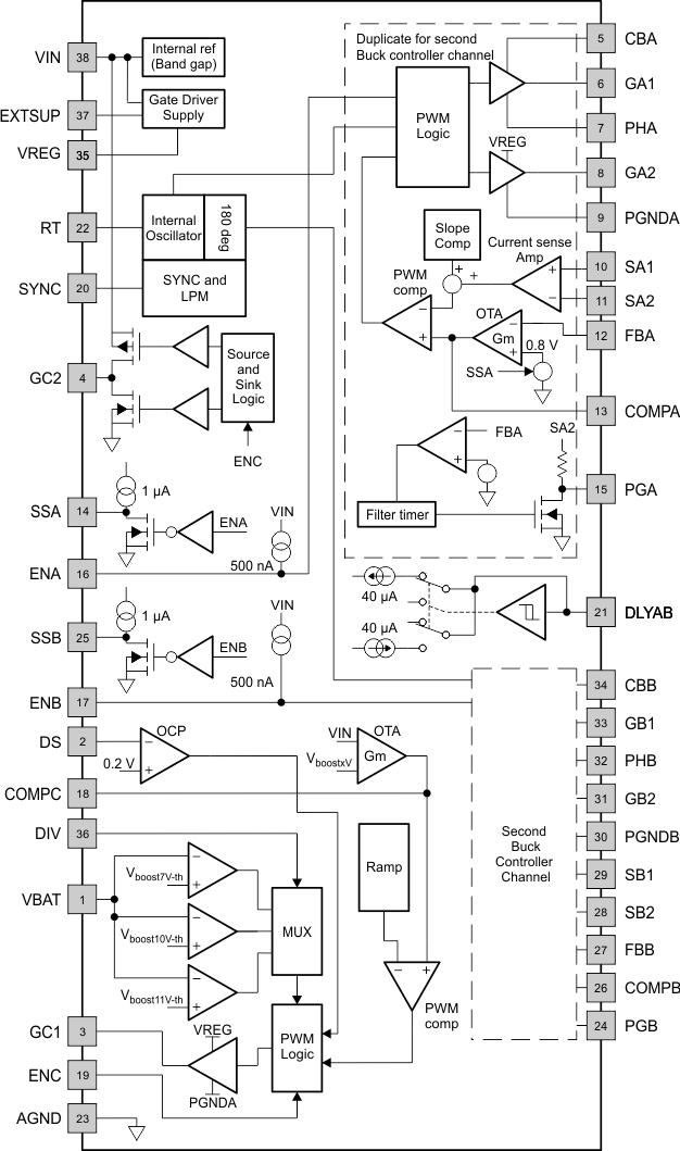
- 6 Pin Configuration and Functions
- 7 Specifications
-
8 Detailed Description
- 8.1 Overview
- 8.2 Functional Block Diagram
- 8.3 Feature Description
- 8.4 Device Functional Modes
-
9 Application and Implementation
- 9.1 Application Information
- 9.2
Typical Application
- 9.2.1 Design Requirements
- 9.2.2
Detailed Design Procedure
- 9.2.2.1 Boost Component Selection
- 9.2.2.2 Boost Maximum Input Current IIN_MAX
- 9.2.2.3 Boost Inductor Selection, L
- 9.2.2.4 Inductor Ripple Current, IRIPPLE
- 9.2.2.5 Peak Current in Low-Side FET, IPEAK
- 9.2.2.6 Right Half-Plane Zero RHP Frequency, fRHP
- 9.2.2.7 Output Capacitor, COUTx
- 9.2.2.8 Bandwidth of Boost Converter, fC
- 9.2.2.9 Output Ripple Voltage Due to Load Transients, ∆VOUTx
- 9.2.2.10 Selection of Components for Type II Compensation
- 9.2.2.11 Input Capacitor, CIN
- 9.2.2.12 Output Schottky Diode D1 Selection
- 9.2.2.13 Low-Side MOSFET (BOT_SW3)
- 9.2.2.14 BuckA Component Selection
- 9.2.2.15 Inductor Selection L
- 9.2.2.16 Inductor Ripple Current IRIPPLE
- 9.2.2.17 Output Capacitor COUTA
- 9.2.2.18 Bandwidth of Buck Converter fC
- 9.2.2.19 Selection of Components for Type II Compensation
- 9.2.2.20 Resistor Divider Selection for Setting VOUTA Voltage
- 9.2.2.21 BuckB Component Selection
- 9.2.2.22 Resistor Divider Selection for Setting VOUT Voltage
- 9.2.2.23 BuckX High-Side and Low-Side N-Channel MOSFETs
- 9.2.3 Application Curves
- 10Power Supply Recommendations
- 11Layout
- 12Device and Documentation Support
- 13Mechanical, Packaging, and Orderable Information
Package Options
Mechanical Data (Package|Pins)
- DAP|38
Thermal pad, mechanical data (Package|Pins)
- DAP|38
Orderable Information
8 Detailed Description
8.1 Overview
The TPS43330-Q1 and TPS43332-Q1 devices include two current-mode synchronous buck controllers and a voltage mode boost controller. The integrated boost controller allows the devices to operate down to 2 V at the input without seeing a drop on the buck regulator output stages. At light loads, one can enable the buck controllers to operate automatically in low-power mode, consuming just 30 μA of quiescent current. The buck controllers have independent soft-start capability and power-good indicators. Current foldback in the buck controllers and cycle-by-cycle current limitation in the boost controller provide external MOSFET protection. The switching frequency is programmable over 150 kHz to 600 kHz or can be synchronized to an external clock in the same range. The TPS43332-Q1 device also offers frequency-hopping spread-spectrum operation.
8.3 Feature Description
8.3.1 Buck Controllers: Normal Mode PWM Operation
8.3.1.1 Frequency Selection and External Synchronization
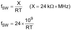
The buck controllers operate using constant-frequency peak-current-mode control for optimal transient behavior and ease of component choices. The switching frequency is programmable between 150 kHz and 600 kHz, depending upon the resistor value at the RT pin. A short circuit to ground at this pin sets the default switching frequency to 400 kHz. Using a resistor at RT sets another frequency according to Equation 1.
For example,
600 kHz requires 40 kΩ
150 kHz requires 160 kΩ
Synchronizing to an external clock at the SYNC pin in the same frequency range of 150 kHz to 600 kHz is also possible. The device detects clock pulses at this pin, and an internal PLL locks on to the external clock within the specified range. The device can also detect a loss of clock at this pin, and upon detection of this condition, the device sets the switching frequency to the internal oscillator. The two buck controllers operate at identical switching frequencies, 180 degrees out-of-phase.
8.3.1.2 Enable Inputs
Independent enable inputs from the ENA and ENB pins enable the buck controllers. The ENx pins are high-voltage pins, with a threshold of 1.7 V for the high level, and with which direct connection to the battery is permissible for self-bias. The low threshold is 0.7 V. Both these pins have internal pullup currents of 0.5 µA (typical). As a result, an open circuit on these pins enables the respective buck controllers. When both buck controllers are disabled, the device shuts down and consumes a current of less than 4 µA.
8.3.1.3 Feedback Inputs
The right-resistor feedback-divider network connected to the FBx (feedback) pins sets the output voltage. Choose this network such that the regulated voltage at the FBx pin equals 0.8 V. The FBx pins have a 100-nA pullup current source as a protection feature in case the pins open up as a result of physical damage.
8.3.1.4 Soft-Start Inputs
To avoid large inrush currents, each buck controller has an independent programmable soft-start timer. The voltage at the SSx pin acts as the soft-start reference voltage. The 1-µA pullup current available at the SSx pins, in combination with a suitably chosen capacitor, generates a ramp of the desired soft-start speed. After startup, the pullup current ensures that SSx is higher than the internal reference of 0.8 V; 0.8 V then becomes the reference for the buck controllers. Use Equation 2 to calculate the soft-start ramp time.
where
- CSS is the required capacitor for ∆t, the desired soft-start time
- ISS = 1 µA (typical)
- ∆V = 0.8 V
An alternative use of the soft-start pins is as tracking inputs. In this case, connect them to the supply to be tracked by a suitable resistor-divider network.
8.3.1.5 Current Sensing and Current Limit With Foldback
Clamping of the maximum value of the COMPx pin limits the maximum current through the inductor to a specified value. When the output of the buck regulator (and hence the feedback value at the FBx pin) falls to a low value because of a short circuit or overcurrent condition, the clamped voltage at the COMPx pin successively decreases, thus providing current foldback protection, which protects the high-side external MOSFET from excess current (forward-direction current limit).
Similarly, if a fault condition shorts the output to a high voltage and the low-side MOSFET turns fully on, the COMPx node drops low. A clamp is on the lower end as well to limit the maximum current in the low-side MOSFET (reverse-direction current limit).
An external resistor senses the current through the inductor. Choose the sense resistor such that the maximum forward peak-current in the inductor generates a voltage of 75 mV across the sense pins. This specified value is for low duty cycles only. At typical duty-cycle conditions around 40% (assuming 5 V output and 12 V input), 50 mV is a more reasonable value, considering tolerances and mismatches. The graphs in the Typical Characteristicssection provide a guide for using the correct current-limit sense voltage.
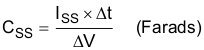
The current-sense pins Sx1 and Sx2 are high-impedance pins with low leakage across the entire output range, thus allowing DCR current sensing using the dc resistance of the inductor for higher efficiency. Figure 16 shows DCR sensing. Here, the series resistance (DCR) of the inductor is the sense element. Place the filter components close to the device for noise immunity. Remember that while the DCR sensing gives high efficiency, it is inaccurate because of the temperature sensitivity and a wide variation of the parasitic inductor series resistance. Therefore using the more-accurate sense resistor for current sensing may be advantageous.
 Figure 16. DCR Sensing Configuration
8.3.1.6 Slope Compensation
Optimal slope compensation, which is adaptive to changes in input voltage and duty cycle, allows stable operation under all conditions. For optimal performance of this circuit, select the inductor and sense resistor according to Equation 3.
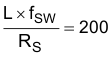
where
- L is the buck-regulator inductor in henries
- fsw is the buck-regulator switching frequency in hertz
- RS is the sense resistor in ohms
8.3.1.7 Power-Good Outputs and Filter Delays
Each buck controller has an independent power-good comparator monitoring the feedback voltage at the FBx pins and indicating whether the output voltage has fallen below a specified power-good threshold. This threshold has a typical value of 93% of the regulated output voltage. The power-good indicator is available as an open-drain output at the PGx pins. An internal 50-kΩ pullup resistor to Sx2 is available, or use of an external resistor is possible. Shutdown of a buck controller causes an internal pulldown of the power-good indicator. Connecting the pullup resistor to a rail other than the output of that particular buck channel causes a constant current flow through the resistor when the buck controller is powered down.
To avoid triggering the power-good indicators because of noise or fast transients on the output voltage, the device uses an internal delay circuit for de-glitching. Similarly, when the output voltage returns to the set value after a long negative transient, assertion of the power-good indicator (release of the open-drain pin) occurs after the same delay. Use of this delay can pause the reset of circuits powered from the buck regulator rail. Program the duration of the delay by using a suitable capacitor at the DLYAB pin according to Equation 4.
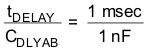
When the DLYAB pin is open, the delay setting is for a default value of 20 µs typical. The power-good delay timing is common to both the buck rails, but the power-good comparators and indicators function independently.
8.3.2 Boost Controller
The boost controller has a fixed-frequency voltage-mode architecture and includes cycle-by-cycle current-limit protection for the external N-channel MOSFET. The boost-controller switching-frequency setting is one-half of the buck-controller switching frequency. An internal resistor-divider network programmable to 7 V, 10 V, or 11 V sets the output voltage of the boost controller at the VIN pin, based on the low, open, or high status, respectively, of the DIV pin. The device does not recognize a change of the DIV setting while the in the low-power mode.
The active-high ENC pin enables the boost controller, which is active when the input voltage at the VBAT pin has crossed the unlock threshold of 8.5 V at least once. A single threshold crossing arms the boost controller, which begins switching as soon as VIN falls below the value set by the DIV pin, regulating the VIN voltage. Thus, the boost regulator maintains a stable input voltage for the buck regulators during transient events such as a cranking pulse at the VBAT pin.
A voltage at the DS pin exceeding 200 mV pulls the CG1 pin low, turning off the boost external MOSFET. Connecting the DS pin to the drain of the MOSFET or to a sense resistor between the MOSFET source and ground achieves cycle-by-cycle overcurrent protection for the MOSFET. Select the on-resistance of the MOSFET or the value of the sense resistor in such a way that the on-state voltage at DS does not exceed 200 mV at the maximum-load and minimum-input-voltage conditions. When using a sense resistor, TI recommends connecting a filter network between the DS pin and the sense resistor for better noise immunity.
The boost output (VIN) can be used to supply other circuits in the system. However, the boost output should be high-voltage tolerant. The device regulates the boost output to the programmed value only when VIN is low, and so VIN can reach battery levels.
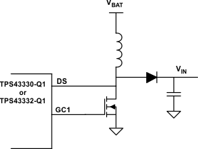 Figure 17. External Drain-Source Voltage Sensing
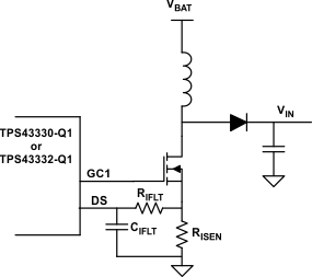 Figure 18. External Current Shunt Resistor
8.3.3 Frequency-Hopping Spread Spectrum
The TPS43332-Q1 device features a frequency-hopping pseudo-random spectrum-spreading architecture. On this device, whenever the SYNC pin is high, the internal oscillator frequency varies from one cycle to the next within a band of ±5% around the value programmed by the resistor at the RT pin. The implementation uses a linear-feedback shift register that changes the frequency of the internal oscillator based on a digital code. The shift register is long enough to make the hops pseudo-random in nature and has a design such that the frequency shifts only by one step at each cycle to avoid large jumps in the buck and boost switching frequencies.
Table 1. Frequency-Hopping Control
8.3.4 Gate-Driver Supply (VREG, EXTSUP)
The gate-driver supplies of the buck and boost controllers are from an internal linear regulator whose output (5.8 V typical) is on the VREG pin and requires decoupling with a ceramic capacitor in the range of 3.3 µF to 10 µF.
NOTE
This pin has internal current-limit protection; do not use it to power any other circuits.
The VIN pin powers the VREG linear regulator by default when the EXTSUP voltage is lower than 4.6 V (typical). If VIN is expected to go to high levels, excessive power dissipation can occur in this regulator, especially at high switching frequencies and when using large external MOSFETs. In this case, powering this regulator from the EXTSUP pin is advantageous, which can have a connection to a supply lower than VIN but high enough to provide the gate drive. When the voltage on the EXTSUP pin is greater than 4.6 V, the linear regulator automatically switches to the EXTSUP pin as the input, to provide this advantage. Efficiency improvements are possible when using one of the switching regulator rails from the TPS4333x-Q1 family of devices or any other voltage available in the system to power the EXTSUP pin. The maximum voltage for application to the EXTSUP pin is 9 V.
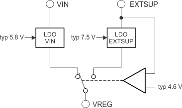 Figure 19. Internal Gate-Driver Supply
Using a voltage above 5.8 V (sourced by VIN) for the EXTSUP pin is advantageous because it provides a large gate drive and hence better on-resistance of the external MOSFETs.
When using the EXTSUP pin, always keep the buck rail supplying the EXTSUP pin enabled. Alternatively, if switching off the buck rail supplying the EXTSUP pin is necessary, place a diode between the buck rail and the EXTSUP pin.
During low-power mode, the EXTSUP functionality is not available. The internal regulator operates as a shunt regulator powered from the VIN pin and has a typical value of 7.5 V. Current-limit protection for the VREG pin is available in low-power mode as well. If the EXTSUP pin is unused, leave the pin open without a capacitor installed.
8.3.5 External P-Channel Drive (GC2) and Reverse-Battery Protection
The TPS4333x-Q1 family of devices include a gate driver for an external P-channel MOSFET which can connect across the rectifier diode of the boost regulator. Such connection is useful to reduce power losses when the boost controller is not switching. The gate driver provides a swing of 6 V typical below the VIN voltage to drive a P-channel MOSFET. When VBAT falls below the boost-enable threshold, the gate driver turns off the P-channel MOSFET, eliminating the diode bypass.
Another use for the gate driver is to bypass any additional protection diodes connected in series, as shown in Figure 20. Figure 21 also shows a different scheme of reverse battery protection, which may require only a smaller-sized diode to protect the N-channel MOSFET, as the diode conducts only for a part of the switching cycle. Because the diode is not always in the series path, the system efficiency can be improved.
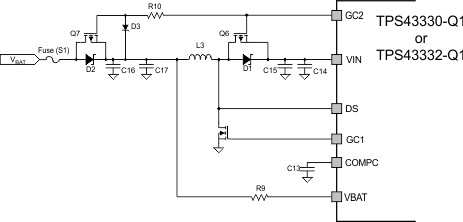 Figure 20. Reverse-Battery Protection Option 1 for Buck-Boost Configuration
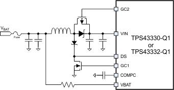 Figure 21. Reverse-Battery Protection Option 2 for Buck-Boost Configuration
8.3.6 Undervoltage Lockout and Overvoltage Protection
The TPS4333x-Q1 family of devices starts up at a VIN voltage of 6.5 V (minimum), required for the internal supply (VREG). When the device has started up, the device operates down to a VIN voltage of 3.6 V; below this voltage level, the undervoltage lockout disables the device.
NOTE
if VIN drops, VREG drops as well and therefore reduces the gate-drive voltage, whereas the digital logic is fully functional. Even if the ENC pin is high, the boost-unlock voltage of typically 8.5 V (typical) one time is required before boost activation can take place (see the Boost Controller section).
A voltage of 46 V at the VIN pin triggers the overvoltage comparator, which shuts down the device. To prevent transient spikes from shutting down the device, the undervoltage and overvoltage protection have filter times of 5 µs (typical).
When the voltages return to the normal operating region, the enabled switching regulators begin including a new soft-start ramp for the buck regulators.
With the boost controller enabled, a voltage less than 1.9 V (typical) on the VBAT pin triggers an undervoltage lockout and pulls the boost gate driver (GC1) low (this action has a filter delay of 5 µs, typical). As a result, VIN falls at a rate dependent on its capacitor and load, eventually triggering VIN undervoltage. A short falling transient at the VBAT pin even lower than 2 V can thus be survived, if VBAT returns above 2.5 V before the VIN pin discharges to the undervoltage threshold.
8.3.7 Thermal Protection
The TPS4333x-Q1 family of devices is protected from overheating using an internal thermal shutdown circuit. If the die temperature exceeds the thermal shutdown threshold of 165ºC because of excessive power dissipation (for example, because of fault conditions such as a short circuit at the gate drivers or the VREG pin), the controllers turn off and then restart when the temperature has fallen by 15ºC.
8.4 Device Functional Modes
Table 2 lists the enable and inhibit pin configurations for the modes of operation.
Table 2. Mode of Operation
| ENABLE AND INHIBIT PINS | DRIVER STATUS | DEVICE STATUS | QUIESCENT CURRENT | ||||
|---|---|---|---|---|---|---|---|
| ENA | ENB | ENC | SYNC | BUCK CONTROLLERS | BOOST CONTROLLER | ||
| Low | Low | Low | X | Shut down | Disabled | Shutdown | Approximately 4 µA |
| Low | High | Low | Low | BuckB running | Disabled | BuckB: LPM enabled | Approximately 30 µA (light loads) |
| High | BuckB: LPM inhibited | mA range | |||||
| High | Low | Low | Low | BuckA running | Disabled | BuckA: LPM enabled | Approximately 30 µA (light loads) |
| High | BuckA: LPM inhibited | mA range | |||||
| High | High | Low | Low | BuckA and BuckB running | Disabled | BuckA and BuckB: LPM enabled | Approximately 35 µA (light loads) |
| High | BuckA and BuckB: LPM inhibited | mA range | |||||
| Low | Low | Low | X | Shut down | Disabled | Shutdown | Approximately 4 µA |
| Low | High | High | Low | BuckB running | Boost running for VIN < set boost output | BuckB: LPM enabled | Approximately 50 µA (no boost, light loads) |
| High | BuckB: LPM inhibited | mA range | |||||
| High | Low | High | Low | BuckA running | Boost running for VIN < set boost output | BuckA: LPM enabled | Approximately 50 µA (no boost, light loads) |
| High | BuckA: LPM inhibited | mA range | |||||
| High | High | High | Low | BuckA and BuckB running | Boost running for VIN < set boost output | BuckA and BuckB: LPM enabled | Approximately 60 µA (no boost, light loads) |
| High | BuckA and BuckB: LPM inhibited | mA range | |||||
8.4.1 Buck Controllers: Current-Mode Operation
Peak-current-mode control regulates the peak current through the inductor to maintain the output voltage at its set value. The error between the feedback voltage at FBx and the internal reference produces a signal at the output of the error amplifier (COMPx) which serves as the target for the peak inductor current. The device senses the current through the inductor as a differential voltage at Sx1–Sx2 and compares voltage with this target during each cycle. A fall or rise in load current produces a rise or fall in voltage at FBx, causing VCOMPx to fall or rise respectively, thus increasing or decreasing the current through the inductor until the average current matches the load. This process maintains the output voltage in regulation.
The top N-channel MOSFET turns on at the beginning of each clock cycle and stays on until the inductor current reaches its peak value. Once this MOSFET turns off, and after a small delay (shoot-through delay) the lower N-channel MOSFET turns on until the start of the next clock cycle. In dropout operation, the high-side MOSFET stays on continuously. In every fourth clock cycle, a limit exists on the duty cycle of 95% to charge the bootstrap capacitor at CBx which allows a maximum duty cycle of 98.75% for the buck regulators. During dropout, the buck regulator switches at one-fourth of the normal frequency.
8.4.2 Buck Controllers: Light-Load PFM Mode
An external clock or a high level on the SYNC pin results in forced continuous-mode operation of the bucks. An open or low on the SYNC pin allows the buck controllers to operate in discontinuous mode at light loads by turning off the low-side MOSFET on detection of a zero-crossing in the inductor current.
In discontinuous mode, as the load decreases, the duration when both the high-side and low-side MOSFETs turn off increases (deep discontinuous mode). In case the duration exceeds 60% of the clock period and VBAT > 8 V, the buck controller switches to a low-power operation mode. The design ensures that this typically occurs at 1% of the set full-load current if the choice of the inductor and sense resistor is as recommended in the slope-compensation section.
In low-power PFM mode, the buck monitors the FBx voltage and compares it with the 0.8-V internal reference. Whenever the FBx value falls below the reference, the high-side MOSFET turns on for a pulse duration inversely proportional to the difference VIN – Sx2. At the end of this on-time, the high-side MOSFET turns off and the current in the inductor decays until it becomes zero. The low-side MOSFET does not turn on. The next pulse occurs the next time FBx falls below the reference value. This results in a constant volt-second ton hysteretic operation with a total device quiescent current consumption of 30 µA when a single buck channel is active and 35 µA when both channels are active.
As the load increases, the pulses become more and more frequent and move closer to each other until the current in the inductor becomes continuous. At this point, the buck controller returns to normal fixed-frequency current-mode control. Another criterion to exit the low-power mode is when VIN falls low enough to require higher than 80% duty cycle of the high-side MOSFET.
The TPS4333x-Q1 family of devices can support the full-current load during low-power mode until the transition to normal mode takes place. The design ensures that exit of the low-power mode occurs at 10% (typical) of full-load current if the selection of inductor and sense resistor is as recommended. Moreover, a hysteresis also exists between the entry and exit thresholds to avoid oscillating between the two modes.
In the event that both buck controllers are active, low-power mode is only possible when both buck controllers have light loads that are low enough for low-power mode entry. With the boost controller enabled, low-power mode is possible only if VBAT is high enough to prevent the boost from switching and if DIV is open or set to GND. A high (VREG) level on DIV inhibits low-power mode, unless the ENC pin is set to low.