SLVSB16E November 2011 – December 2015 TPS43340-Q1
PRODUCTION DATA.
- 1 Features
- 2 Applications
- 3 Description
- 4 Revision History
- 5 Pin Configuration and Functions
- 6 Specifications
-
7 Detailed Description
- 7.1 Overview
- 7.2 Functional Block Diagram
- 7.3 Feature Description
- 7.4 Device Functional Modes
- 8 Application and Implementation
- 9 Power Supply Recommendations
- 10Layout
- 11Device and Documentation Support
- 12Mechanical, Packaging, and Orderable Information
Package Options
Mechanical Data (Package|Pins)
- PHP|48
Thermal pad, mechanical data (Package|Pins)
- PHP|48
Orderable Information
7 Detailed Description
7.1 Overview
The TPS43340-Q1 is a dual-buck regulator controller (Buck1, Buck2), single-buck regulator converter (Buck3) and linear regulator (LREG1) designed for powering the Texas Instruments family of DSPs and microcontrollers or general-market MCU products. The device features integrated short-circuit and overcurrent protection on the gate-drive outputs for the buck regulator controllers and independent current-foldback control for each buck regulator supply during regulator output short to ground. Each output supply incorporates a soft start to ensure that on initial power up these regulated outputs are not in current limit. Implementation of reset delay on power up allows the outputs of Buck1, Buck2, Buck3 and the linear regulator to get to stable regulation. An external capacitor sets the delay to a maximum range of 300 ms. Each power-supply output has adjustable output voltage based on the external resistor-network settings. The device has sequencing control during power up and power down of the output rails, based on the enable-and-disable control or soft start.
7.2 Functional Block Diagram
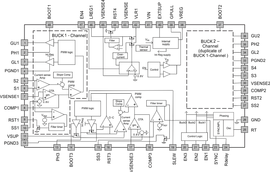 Figure 14. Internal Functional Blocks
7.3 Feature Description
7.3.1 Enable Inputs
The use of independent enable inputs at the EN1 through EN4 pins enables all the regulators. These pins have internal pullup currents of 0.5 µA (typical). As a result, an open circuit on any of these pins enables its respective regulator. EN1, EN2, and EN4 are high-voltage pins, which permits their connection directly to the battery for self-bias. When all regulators are disabled, the device shuts down and consumes a current of 5 µA typical.
7.3.2 Linear Regulator (LREG1)
The linear regulator is an NMOS output low-dropout regulator with output load current up to 300 mA. It can operate directly from the battery. With EN4 tied high or open, LREG1 turns on its output following an internally generated soft-start ramp. The regulation loop uses internal frequency compensation. If the output shorts to ground, the device protects itself by limiting the current. For VIN lower than 9 V, LREG1 controls the internal charge pump depending on VIN and the load current in accordance with Table 4. An internal voltage selector selects the higher available supply, VIN or the charge pump voltage, for the error amplifier. The device monitors the output voltage of the low-dropout regulator for undervoltage and signals its state on pin RST4.
7.3.3 Gate-Driver Supply (VREG, EXTSUP)
An internal linear regulator supplies the gate drivers of the buck controllers and the buck converter. The regulator output (5.8 V typical) is available at the VREG pin and requires decoupling using a ceramic capacitor in the range of 3.3 µF to 10 µF. This pin has an internal current-limit protection; do not use it to power any other circuits.
Power for the VREG linear regulator comes from VIN by default when the EXTSUP voltage is lower than 4.6 V (typical). Should there be an expectation of VIN going to high levels, there can be excessive power dissipation in this regulator, especially at high switching frequencies and when using large external MOSFETs. In this case, it is advantageous to power this regulator from the EXTSUP pin, connection to which can be to a supply lower than VIN but high enough to provide the gate drive. The voltage on EXTSUP should not exceed 9 V. With EXTSUP connected to a voltage greater than 4.6 V, the linear regulator automatically switches to EXTSUP. Efficiency improvements are thus possible when using one of the switching regulator rails from the TPS43340-Q1 or any other voltage available in the system to power the EXTSUP. If the EXTSUP supply is above 4.6 V but below 7.5 V, the EXTSUP-LDO acts as a pass element, providing EXTSUP voltage less a small dropout to VREG.
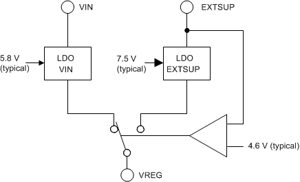 Figure 15. Internal Gate-Driver Supply
Using a voltage above 5.8 V (sourced by VIN) for EXTSUP is advantageous, as it provides a large gate drive and hence better on-resistance of the external MOSFETs.
When using EXTSUP, always keep the buck rail supplying EXTSUP enabled. Alternatively, if it is necessary to switch off the buck rail supplying EXTSUP, place a diode between the buck rail and EXTSUP.
During low-power mode, the EXTSUP functionality is not available. The internal regulator operates as a shunt regulator powered from VIN and has a typical value of 7.5 V. Current-limit protection for VREG is available in low-power mode as well. If EXTSUP is unused, leave the pin open without a capacitor installed.
7.3.4 External P-Channel Drive (GPULL) and Reverse Battery Protection
The TPS43340-Q1 includes a gate driver for an external P-channel MOSFET which can be used for reverse battery protection. This is useful to reduce the voltage drop across the protection element compared to using a series diode to VIN. The gate – source voltage of the external PMOS is clamped by an internal Zener diode to
17 V typical.
| VBAT ≤ VF → | VGS | = 0 V → FET and diode not conducting VF ≤ VBAT ≤ VT (FET) → | VGS | = VBAT → FET NOT conducting and diode conducting VT (FET) ≤ VBAT ≤ 17 V → | VGS | = VBAT → FET conducting VBAT ≥ 17 V → | VGS | = 17 V → FET conducting |
Spacer
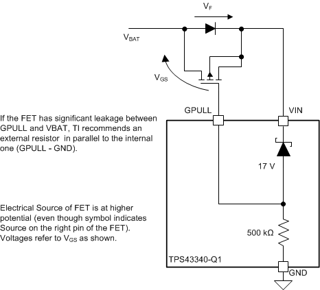 Figure 16. Internal Circuit of GPULL Output
NOTE
An implementation without the PMOS blocks the current coming from Buck-outputs (improper OR-ing, and others), which may result in exceeding the absolute maximum ratings.
7.3.5 Undervoltage Lockout and Overvoltage Protection
The TPS43340-Q1 starts up at a VIN voltage of 6.5 V (maximum). Once it has started up, the device operates down to a VIN undervoltage lockout level of 3.6 V or until reaching a VREG undervoltage of 3.6 V. A voltage above 46 V at VIN shuts down the device. In order to prevent transient spikes from shutting down the device, the under- and overvoltage protection have filter times of 5 µs (typical). There is no support for overvoltage protection in LPM.
When the voltages return to the normal operating region, the enabled regulators start up with a soft-start ramp.
7.3.6 Synchronous Buck Converter Buck3
This regulator operates with the switching frequency set on the RT terminal or an external clock input on the SYNC terminal. The internal power FETs switch out of phase to regulate the output voltage, operating in a pulse width modulation. The converter uses a peak-current mode-control loop with external frequency compensation. The synchronous operation mode improves the overall efficiency.
7.3.6.1 Soft Start and Foldback Functions
A capacitor on the SS3 terminal sets the converter soft start. Pulling the enable pin on EN3 high activates soft start. During soft start or whenever the voltage on VSENSE3 falls below limits given by ƒSW-f-back, the converter switches to a frequency foldback of ƒsw / 2 to help control the coil current. In addition to the frequency foldback, implementation of current foldback reduces power dissipation to protect the converter against an output short to ground. Like in the buck controllers, the current foldback reduces the maximum peak current limit depending on the voltage on the VSENSE3 pin. Figure 9 shows the characteristic of current foldback.
7.3.6.2 Current-Mode Control and Current-Limit Protection
Measurement of the coil peak current is by use of the high-side integrated FET; peak-current regulation occurs in each switching cycle in accordance with the voltage on the COMP3 pin. COMP3 is the output of a transconductance error amplifier of the voltage feedback loop for Buck3, as COMP1 and COMP2 are for controllers Buck1 and Buck2. COMP3 sets the target for the peak current comparator (inner current loop) and serves as frequency compensation of the voltage loop using a type II compensation network.
Clamping the voltage on the COMP3 node realizes the positive current limit. The positive clamping level depends on the voltage on the VSENSE3 pin, as described previously. The device also implements clamping for low voltage on the COMP3 pin, thereby speeding up the transient response after output overshoot. For stability of the current loop, during the switching cycle the internal slope compensation adjusts the current limit set by COMP3.
For correct operation of the slope compensation, the coil used for Buck3 must satisfy the following:
where
- LBuck3 is the inductance in henries
- ƒsw is the switching frequency in hertz
Reaching the positive current limit during the high PWM phase resets the PWM. The high-side FET turns off and the low part of the cycle is initiated. On detecting an overcurrent condition such as an output short to a supply during the PWM low phase, the low-side FET turns off until the end of the given cycle, to allow the coil current to flow through the body diode of the high-side FET.
7.3.6.3 Operation in Dropout and Undervoltage Protection
This converter is capable of operating with a low input-to-output voltage difference. In dropout operation, the integrated high-side MOSFET stays on continuously. In every fourth clock cycle, the device limits the duty cycle to 95% in order to charge the bootstrap capacitor at BOOT3. This allows a maximum duty cycle of 98.75% for the buck converter. In this mode, the output tracks the input until initiation of the internal undervoltage lockout due to low supply voltage on the VSUP pin.
Thermal shutdown monitors the virtual junction temperature of the integrated FETs. When TJ exceeds 170°C, both the high- and low-side switches turn off. The converter returns to normal operation when the temperature decreases to the acceptable level (typically TJ = 150°C)
7.3.6.4 Slew Rate Control (SLEW)
The setting on the SLEW terminal controlss the slew for Buck3. Setting the slew rate to logic high (slowest slew rate) extends the minimum on-time of the buck converter by 5% of the clock period.
| SLEW TERMINAL SETTING | tr (TYP) ns | tf (TYP) ns |
|---|---|---|
| SLEW > VREG – 0.2 V (low slew rate, logic high) | 24 | 7 |
| SLEW pin open – medium slew rate | 11 | 3 |
| SLEW < 0.2 V (fast slew rate, logic low) | 8 | 2 |
7.4 Device Functional Modes
7.4.1 Buck Controllers: Normal Mode PWM Operation
7.4.1.1 Setting the Operating Frequency
The buck controllers operate using constant-frequency peak-current-mode control for optimal transient behavior and ease of component choices. The switching frequency is programmable between 150 kHz and 600 kHz, depending on the resistor value at the RT pin. Tying this pin to ground sets the default switching frequency to 400 kHz. A resistor connected to RT can also set the frequency according to the formula:
where
- 600 kHz requires 40 kΩ
- 150 kHz requires 160 kΩ
It is also possible to synchronize to an external clock at the SYNC pin in the same frequency range of 150 kHz to 600 kHz. The device detects clock pulses at this pin, and an internal PLL locks onto the external clock within the specified range. The device can also detect a loss of clock at this pin, and detection of clock loss for tSW-Trans-delaysets the switching frequency to the internal oscillator. The two buck controllers operate at the same switching frequency, 180 degrees out of phase.
7.4.1.2 Feedback Inputs
Choose the resistor feedback divider networks connected to the VSENSEx (feedback) pins to set the output voltages. Make the choice such that the regulated voltages at the VSENSEx pins equal 0.8 V. The VSENSEx pins have 100-nA pullup current sources as a protection feature in case the pins open up as a result of physical damage.
7.4.1.3 Soft-Start Inputs
In order to avoid large inrush currents, both buck controllers have independent programmable soft-start timing. The voltage at the SSx pins acts as the soft-start reference voltage. A 1-µA pullup current is available at the SSx pins, and by choosing a suitable capacitor one can obtain a desired soft-start ramp speed. After start-up, the pullup current ensures that pins SSx are higher than the internal reference of 0.8 V, which then becomes the reference for the buck controllers. The required capacitor for ∆t, the desired soft-start time, is given by:

where
- ISS = 1 µA (typical)
- ∆V = 0.8 V
Alternatively, one can use the soft-start pins as tracking inputs. In this case, connect the pins to the supply to be tracked via a suitable divider network.
7.4.1.4 Current-Mode Operation
Peak current-mode control regulates the peak current through the inductor such that the output voltage maintains its set value. The error between the feedback voltage at VSENSEx and the internal reference produces a signal at the output of the error amplifier (COMPx) which serves as the target for the peak inductor current. This target provides a comparison for the current through the inductor, sensed as a differential voltage at S1-S2 for Buck1 and S3-S4 for Buck2, and compared with this target during each cycle. A fall or rise in load current produces a rise or fall in voltage at VSENSEx, causing COMPx to fall or rise, respectively, thus increasing or decreasing the current through the inductor until the average current matches the load. In this way, the device maintains the output voltage in regulation.
The high-side N-channel MOSFET turns on at the beginning of each clock cycle and remains on until the inductor current reaches its peak value. Once this MOSFET turns off, and after a small delay (shoot-through delay), the lower N-channel MOSFET turns on until the start of the next clock cycle. In dropout operation, the high-side MOSFET stays on continuously. In every fourth clock cycle, the duty cycle is limited to 95% in order to charge the bootstrap capacitor at BOOTx. This allows a maximum duty cycle of 98.75% for the buck regulators. Thus, during dropout the buck regulators switch at one-fourth of the normal frequency.
7.4.1.5 Current Sensing and Current Limit With Foldback
Clamping the maximum value of COMPx is such as to limit the maximum current through the inductor to a specified value. When the output of the buck regulator (and hence the feedback value at VSENSEx) falls to a low value due to a short circuit or overcurrent condition, the clamping voltage at the COMPx successively decreases, thus providing current foldback protection. This protects the high-side external MOSFET from excess current (forward-direction current limit).
Similarly, if due to a fault condition the output shorts to a high voltage and turns the low-side MOSFET fully on, the COMPx node drops low. The device holds COMPx at a low level as well in order to limit the maximum current in the low-side MOSFET (reverse direction current limit).
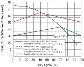
An external resistor senses the current through the inductor. Choose the sense resistor such that the maximum forward peak current in the inductor generates a voltage of 75 mV across the sense pins. This value specification is at low duty cycles only. At typical duty cycle conditions around 40% (assuming 5-V output and 12-V input), 50 mV is a more reasonable value, considering the slope compensation and tolerances. The typical characteristics in Figure 18 and Figure 12 provide a guide for using the correct current-limit sense voltage.
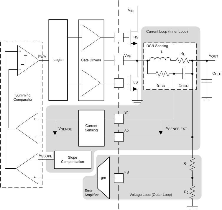
The current-sense pins Sx are high-impedance pins with low leakage across the entire output range. These pin characteristics allow DCR current sensing using the dc resistance of the inductor for higher efficiency. Figure 17 shows DCR sensing. Here the series resistance (DCR) of the inductor serves as the sense element. Place the filter components close to the device for noise immunity. Remember that while DCR sensing gives high efficiency, it is less accurate due to the temperature sensitivity and a wide variation of the parasitic series resistance of the inductor. Hence, it may often be advantageous to use the more-accurate sense resistor for current sensing.
7.4.1.6 Slope Compensation
Optimal slope compensation which is adaptive to changes in input voltage and duty cycle allows stable current-mode operation in all conditions. For optimal performance of this circuit, satisfy the following condition in the choice of inductor and sense resistor:

where
- L is the buck regulator inductor in henries
- RS is the sense resistor in ohms
- fsw is the buck regulator switching frequency in Hz
7.4.1.7 Reset Outputs and Filter Delays
Each buck controller has an independent reset comparator monitoring the feedback voltage at the VSENSEx pins and indicating whether the output voltage has fallen below the specified reset threshold. The reset indicator is available as an open-drain output at the RSTx pins. An internal 50-kΩ pullup resistor to S2 or S4 is available, or one can use an external resistor. When a buck controller shuts down, the device pulls down the power-good outputs internally. Connecting the pullup resistor to a rail other than the output of that particular buck channel causes a constant current flow through the resistor when the buck controller powers down.
In order to avoid triggering the power-good indicators due to noise or fast transients on the output voltage, the device implements an internal delay of tdeglitch for de-glitching. The output voltage reaching its set value after a start-up ramp or negative transient asserts the power-good indicator high (releases the open-drain pin) after a delay of tdelay, at least tdelay_fix. A use of this is to delay the reset to the circuits being powered from the buck regulator rail. Program the delay of this circuit by using a suitable capacitor at the Rdelay pin according to Equation 6:
Power-Good Output Delay

where
- CRdelay is the capacitor value in farads on the Rdelay pin.
An open on the Rdelay pin sets the delay to a default value of 20 µs typical. The power-good delay timing is common to all supply rails, but the power good comparators and outputs function independently.
7.4.1.8 Light-Load PFM Mode
An external clock or a high level on the SYNC pin or enabling Buck3 results in forced continuous-mode operation of the bucks. Having the SYNC pin low or open allows the buck controllers to operate in discontinuous mode at light loads by turning off the low-side MOSFET on detection of a zero-crossing in the inductor current.
In discontinuous mode, as the load decreases, the duration of the clock period when both the high-side and the low-side MOSFETs are turned off increases (deep discontinuous mode). In case the duration exceeds 60% of the clock period and VIN > 8 V, the buck controller switches to a low-power operation mode. The design ensures that this typically occurs at 1% of the set full-load current if the choice of the inductor and the sense resistor is appropriate as recommended in the slope compensation section.
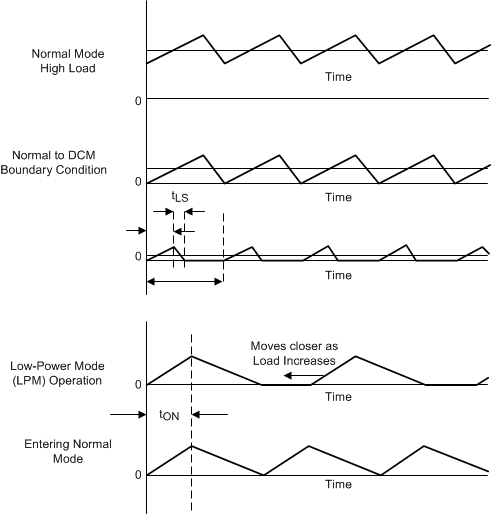 Figure 19. Modes of Operation
In low-power PFM mode, the buck controllers monitor the VSENSEx voltage and compare it with the 0.8 V internal reference. Whenever the VSENSEx value falls below the reference, the high-side MOSFET turns on for a pulse-duration inversely proportional to the difference across VIN-S2 for Buck 1 and VIN-S4 for Buck2. At the end of this on-time, the high-side MOSFET turns off and the current in the inductor decays until it becomes zero. The low-side MOSFET does not turn on. The next pulse occurs the next time VSENSEx falls below the reference value. This results in a constant volt-second TON hysteretic operation with a total device quiescent current consumption of 30 µA when a single buck channel is active and 35 µA when both channels are active.
As the load increases, the pulse become more and more frequent until the current in the inductor becomes continuous. At this point, the buck controller returns to normal fixed-frequency current-mode control. Another criterion for exit from the low-power mode is when VIN falls low enough to require a higher-than-80% duty cycle of the high-side MOSFET.
The TPS43340-Q1 can support the full-current load during low-power mode until the transition to normal mode takes place. The design ensures the low-power-mode exit occurs at 10% (typical) of full-load current if the inductor and sense resistor choices are as recommended. Moreover, there is always a hysteresis between the entry and exit thresholds to avoid oscillating between the two modes.
In the event that both buck controllers are active, low-power mode is only possible when both buck controllers have light loads that are low enough for entry to low-power mode.

