SLUS609J May   2004  – January 2018 TPS51116

PRODUCTION DATA.  

  1. Features
  2. Applications
  3. Description
    1.     Device Images
      1. 3.1 Typical Application
  4. Revision History
  5. Pin Configuration and Functions
    1.     Pin Functions
  6. Specifications
    1. 6.1 Absolute Maximum Ratings
    2. 6.2 ESD Ratings
    3. 6.3 Recommended Operating Conditions
    4. 6.4 Dissipation Ratings
    5. 6.5 Thermal Information
    6. 6.6 Electrical Characteristics
    7. 6.7 Typical Characteristics
  7. Detailed Description
    1. 7.1 Overview
    2. 7.2 Functional Block Diagram
    3. 7.3 Feature Description
      1. 7.3.1  VDDQ SMPS, Light Load Condition
      2. 7.3.2  Low-Side Driver
      3. 7.3.3  High-Side Driver
      4. 7.3.4  Current Sensing Scheme
      5. 7.3.5  PWM Frequency and Adaptive On-Time Control
      6. 7.3.6  VDDQ Output Voltage Selection
      7. 7.3.7  VTT Linear Regulator and VTTREF
      8. 7.3.8  Controling Outputs Using the S3 and S5 Pins
      9. 7.3.9  Soft-Start Function and Powergood Status
      10. 7.3.10 VDDQ and VTT Discharge Control
      11. 7.3.11 Current Protection for VDDQ
      12. 7.3.12 Current Protection for VTT
      13. 7.3.13 Overvoltage and Undervoltage Protection for VDDQ
      14. 7.3.14 Undervoltage Lockout (UVLO) Protection, V5IN (PWP), V5FILT (RGE)
      15. 7.3.15 Input Capacitor, V5IN (PWP), V5FILT (RGE)
      16. 7.3.16 Thermal Shutdown
    4. 7.4 Device Functional Modes
      1. 7.4.1 VDDQ SMPS, Dual PWM Operation Modes
      2. 7.4.2 Current Mode Operation
      3. 7.4.3 D-CAP™ Mode Operation
  8. Application and Implementation
    1. 8.1 Application Information
    2. 8.2 DDR3 Application With Current Mode
      1. 8.2.1 Design Requirements
      2. 8.2.2 Detailed Design Procedure
        1. 8.2.2.1 Pin Connections
        2. 8.2.2.2 Choose the inductor
        3. 8.2.2.3 Choose rectifying (low-side) MOSFET
        4. 8.2.2.4 Choose output capacitance
        5. 8.2.2.5 Determine f0 and calculate RC
        6. 8.2.2.6 Calculate CC2
        7. 8.2.2.7 Calculate CC.
        8. 8.2.2.8 Determine the value of R1 and R2.
      3. 8.2.3 Application Curves
    3. 8.3 DDR3 Application With D−CAP™ Mode
      1. 8.3.1 Design Requirements
      2. 8.3.2 Detailed Design Procedure
        1. 8.3.2.1 Pin Connections
        2. 8.3.2.2 Choose the Components
      3. 8.3.3 Application Curves
  9. Power Supply Recommendations
  10. 10Layout
    1. 10.1 Layout Guidelines
    2. 10.2 Layout Example
  11. 11Device and Documentation Support
    1. 11.1 Receiving Notification of Documentation Updates
    2. 11.2 Community Resources
    3. 11.3 Trademarks
    4. 11.4 Electrostatic Discharge Caution
    5. 11.5 Glossary
  12. 12Mechanical, Packaging, and Orderable Information

Package Options

Refer to the PDF data sheet for device specific package drawings

Mechanical Data (Package|Pins)
  • RGE|24
  • PWP|20
Thermal pad, mechanical data (Package|Pins)
Orderable Information

Typical Characteristics

All data in the following graphs are measured from the PWP packaged device.
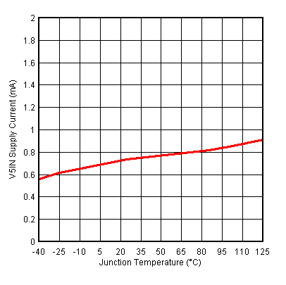
TPS51116 D024_SLUS609.gif
Figure 1. V5IN Supply Current vs Junction Temperature
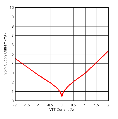
TPS51116 D023_SLUS609.gif
DDR2 VVTT = 0.3 V
Figure 3. V5IN Supply Current vs VTT Current
TPS51116 icsvst_lus609.gif
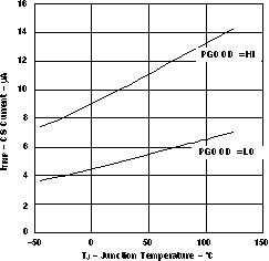
Figure 5. CS Current vs Junction Temperature
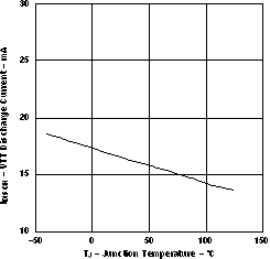
TPS51116 idschavst_lus609.gif
Figure 7. VTT Discharge Current vs Junction Temperature
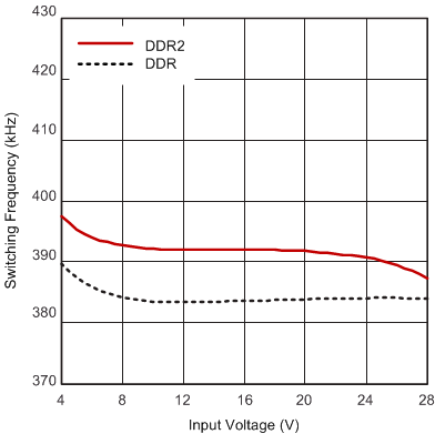
TPS51116 fswvsvin_slus609.gif
DCAP Mode IVDDQ = 7 A
Figure 9. Switching Frequency vs Input Voltage
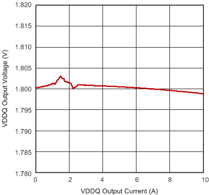
TPS51116 vvddqvsivddq_slus609.gif
DDR VIN = 12 V
DCAP Mode
Figure 11. VDDQ Load Regulation
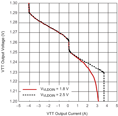
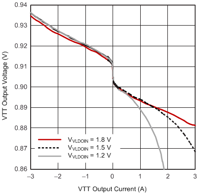
TPS51116 vvttvsivtta_slus609.gif
DDR
Figure 13. VTT Load Regulation
TPS51116 D012_SLUS609.gif
DDR3 VVLDOIN = 1. 5 V
Figure 15. VTT Load Regulation
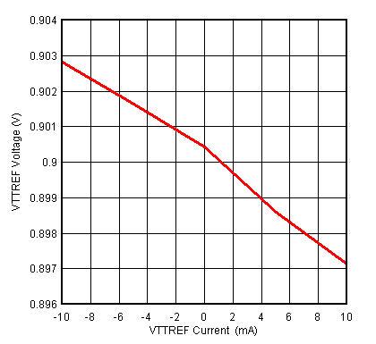
TPS51116 D021_SLUS609.gif
DDR D021
Figure 17. VTTREF Load Regulation
TPS51116 D011_SLUS609.gif
DDR3
Figure 19. VTTREF Load Regulation
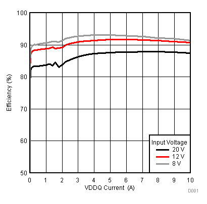
TPS51116 D026_SLUS609.gif
DDR VVDDQ = 2.5 V
fSW = 400 kHz
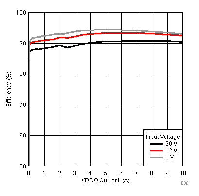
Figure 21. VDDQ Efficiency vs VDDQ Current
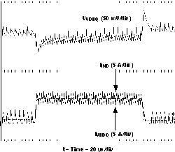
TPS51116 ripple_lus609.gif
Heavy Load
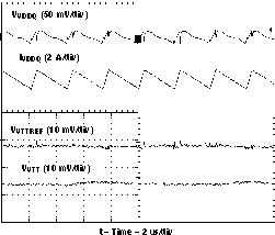
Figure 23. Ripple Waveforms
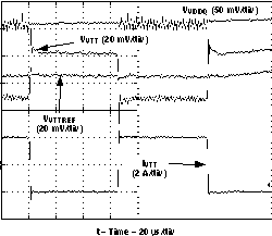
TPS51116 vttload_lus609.gif
Figure 25. VTT Load Transient Response
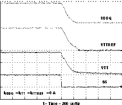
TPS51116 sswtrack_lus609.gif
Figure 27. Soft-Start Waveforms Tracking Discharge
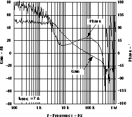
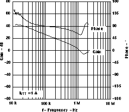
TPS51116 vddqbode_lus609.gif
Current mode
Figure 29. VDDQ Bode Plot
TPS51116 bodesink_lus609.gif
DDR2 Sink
Figure 31. VTT Bode Plot
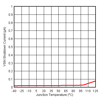
TPS51116 D025_SLUS609.gif
Figure 2. V5IN Shutdown Current vs Junction Temperature
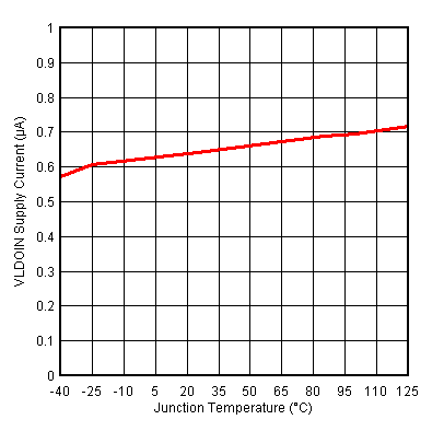
TPS51116 D028_SLUS609.gif
Figure 4. VLDOIN Supply Current vs Junction Temperature
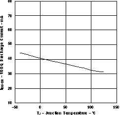
TPS51116 idschbvst_lus609.gif
Figure 6. VDDQ Discharge Current vs Junction Temperature
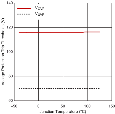
TPS51116 ouvptripvt_lus609.gif
Figure 8. Overvoltage and Undervoltage Threshold vs Junction Temperature
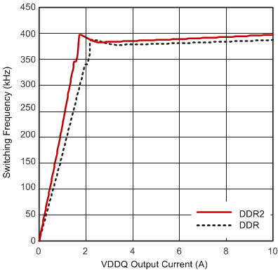
TPS51116 fswvsivddq_slus609.gif
DCAP Mode VIN =12 V
Figure 10. Switching Frequency vs IVDDQ Output Current
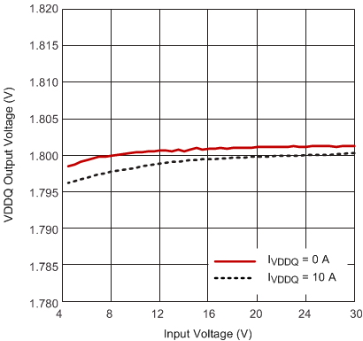
TPS51116 vvddqvsvin_slus609.gif
DDR2 DCAP Mode
Figure 12. VDDQ Line Regulation
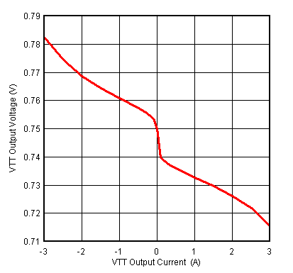
TPS51116 vvttvsivttb_slus609.gif
DDR2
Figure 14. VTT Load Regulation
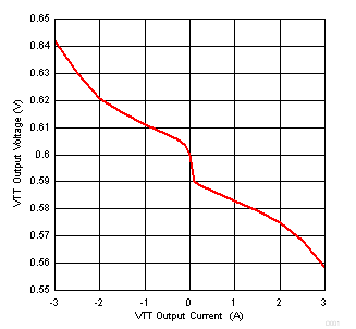
TPS51116 D002_SLUS609.gif
DDR4
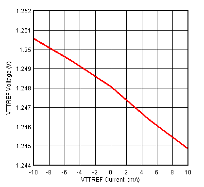
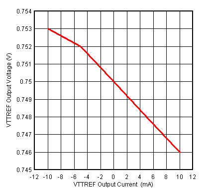
Figure 16. VTTREF Output Voltage vs Output Current
TPS51116 D022_SLUS609.gif
DDR2
Figure 18. VTTREF Load Regulation
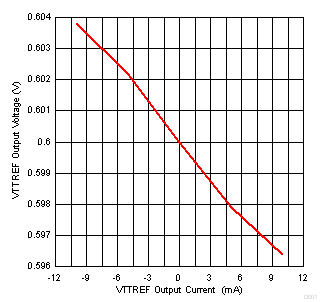
TPS51116 D003_SLUS609.gif
DDR4
Figure 20. VTTREF Load Regulation
TPS51116 D027_SLUS609.gif
DDR2 VVDDQ = 1.8 V
fSW = 400 kHz
Figure 22. VDDQ Efficiency vs VDDQ Current
TPS51116 transient_lus609.gif
Figure 24. VDDQ Load Transient Response
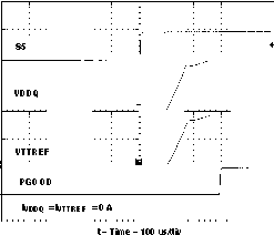
TPS51116 startup_lus609.gif
Figure 26. VDDQ, VTT, and VTTREF Start-Up Waveforms
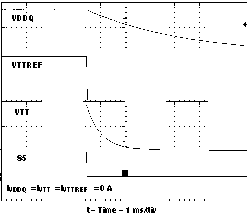
TPS51116 sswotrack_lus609.gif
Figure 28. Soft-Stop Waveforms Non-Tracking Discharge
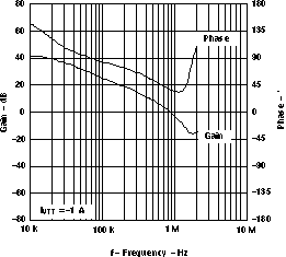
TPS51116 bodesource_lus609.gif
DDR2 Source
Figure 30. VTT Bode Plot