SLVS631C December 2005 – May 2015 TPS51117
PRODUCTION DATA.
- 1 Features
- 2 Applications
- 3 Description
- 4 Revision History
- 5 Pin Configuration and Functions
- 6 Specifications
-
7 Detailed Description
- 7.1 Overview
- 7.2 Functional Block Diagram
- 7.3
Feature Description
- 7.3.1 PWM Frequency and Adaptive On-Time Control
- 7.3.2 Low-Side Driver
- 7.3.3 High-Side Driver
- 7.3.4 Soft-Start
- 7.3.5 Powergood
- 7.3.6 Output Discharge Control (Soft-Stop)
- 7.3.7 Overcurrent Limit
- 7.3.8 Negative Overcurrent Limit (PWM-Only Mode)
- 7.3.9 Overvoltage Protection
- 7.3.10 Undervoltage Protection
- 7.3.11 Start-Up Sequence
- 7.3.12 UVLO Protection
- 7.3.13 Thermal Shutdown
- 7.4 Device Functional Modes
- 8 Application and Implementation
- 9 Power Supply Recommendations
- 10Layout
- 11Device and Documentation Support
- 12Mechanical, Packaging, and Orderable Information
Package Options
Refer to the PDF data sheet for device specific package drawings
Mechanical Data (Package|Pins)
- RGY|14
- PW|14
Thermal pad, mechanical data (Package|Pins)
- RGY|14
Orderable Information
8 Application and Implementation
NOTE
Information in the following applications sections is not part of the TI component specification, and TI does not warrant its accuracy or completeness. TI’s customers are responsible for determining suitability of components for their purposes. Customers should validate and test their design implementation to confirm system functionality.
8.1 Application Information
The TPS51117 is a cost-effective, synchronous buck controller for POL voltage regulation in notebook PC applications. The controller is dedicated for Adaptive On-Time D-CAP Mode operation. Use the following design procedure to select component values for each device.
8.2 Typical Application
A buck converter system using D-CAP Mode can be simplified as shown in Figure 21.
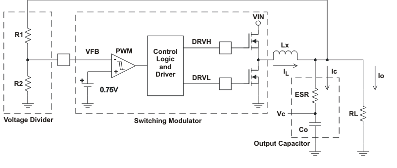 Figure 21. Simplified Diagram of the Modulator
8.2.1 Design Requirements
For this design example, use Table 1 as the input parameters.
Table 1. Design Parameters
| DESIGN PARAMETER | EXAMPLE VALUE | |||
|---|---|---|---|---|
| Input Voltage Range | 1.8 V to 28 V | |||
| Output Voltage | 1.05 V | |||
| Output Current Rating | 10 A | |||
8.2.2 Detailed Design Procedure
8.2.2.1 D-CAP Mode Operation
The VFB voltage is compared with the internal reference voltage after the divider resistors. The PWM comparator determines the timing to turn on the top MOSFET. The gain and speed of the comparator is high enough to keep the voltage at the beginning of each on cycle (or the end of off cycle) substantially constant. The DC output voltage may have line regulation due to ripple amplitude that slightly increases as the input voltage increases.
For loop stability, the 0 dB frequency, f0, defined in Equation 6 must be lower than 1/4 of the switching frequency.

As f0 is determined solely by the output capacitor characteristics, loop stability of D-CAP Mode is determined by capacitor chemistry. For example, specialty polymer capacitors (SP-CAP) have Co in the order of several 100 μF and ESR in range of 10 mΩ. These values make f0 in the order of 100 kHz or less and the loop is stable. However, ceramic capacitors have f0 at more than 700 kHz, which is not suitable for this operational mode.
Although D-CAP Mode provides many advantages such as ease-of-use, minimum external component configuration, and extremely short response time, due to not employing an error amplifier in the loop, a sufficient feedback signal must be provided by an external circuit to reduce the jitter level. The required signal level is approximately 15 mV at the comparing point. This generates Vripple = (VOUT/0.75) × 15 mV at the output node. The output capacitor ESR should meet this requirement.
The external component selection is simple in D-CAP Mode:
- Determine the value of R1 and R2
- Choose RTON
- Choose inductor
- Choose output capacitor(s)
- Choose MOSFETs
- Choose Rtrip
- LPF for V5FILT
- VBST capacitor, VBST diode
The recommended R2 value is 10 kΩ to 100 kΩ. Calculate R1 by Equation 7.

Switching frequency is usually determined by the overall view of the DC-DC converter design of: size, efficiency or cost, and mostly dictated by external component constraints such as the size of inductor and/or output capacitor. When an extremely low or high duty factor is expected, the minimum on-time or off-time also must be considered to satisfy the required duty factor. Once the switching frequency is decided, RTON can be determined by Equation 8 and Equation 9,


A good starting point inductance value is where the ripple current is approximately 1/4 to 1/2 of the maximum output current.

For applications that require fast transient response with minimum VOUT overshoot, consider a smaller inductance than above. The cost of a small inductance value is higher steady-state ripple, larger line regulation, and higher switching loss.
The inductor also needs to have low DCR to achieve good efficiency, as well as enough room above peak inductor current before saturation. The peak inductor current can be estimated in Equation 11.

Organic semiconductor capacitor(s) or specialty polymer capacitor(s) are recommended. Determine ESR to meet the required ripple voltage above. A quick approximation is shown in Equation 12.

Loss-less current sensing and overcurrent protection of the TPS51117 is determined by RDS(on) of the low-side MOSFET. So, RDS(on) times the inductor current value at the overcurrent point should be in the range of 30 mV to 200 mV for the entire operational temperature range. Assuming a 20% guard band, RDS(on) in Equation 13 should satisfy the full temperature range.

Once the low-side FET is decided, select an appropriate Rtrip value that provides Vtrip equal to RDS(on) times Ipeak.
To reject high-frequency noise and also secure safe start-up of the internal reference circuit, apply 1 μF of MLCC closely at the V5FILT pin with a 300-Ω resistor to create a LPF between +5-V supply and the pin.
Apply 0.1-μF MLCC between VBST and the LL node as the flying capacitor for the high-side FET driver. The TPS51117 has its own boost diode onboard between V5DRV and VBST. This is a PN junction diode and strong enough for most typical applications. However, in case efficiency has priority over cost, the designer may add a Schottky diode externally to improve gate drive voltage of the high-side FET. A Schottky diode has a higher leakage current, especially at high temperature, than a PN junction diode. A low-leakage diode should be selected in order to maintain VBST voltage during low-frequency operation in skip mode.
Table 2. Typical Application Circuit Components
| SYMBOL | SPECIFICATION | MANUFACTURER | PART NUMBER |
|---|---|---|---|
| C1A, C1B | 470 μF, 2.5 V, 12 mΩ | SANYO | 2R5TPE470MC |
| C2 | 10 μF, 25 V, 2 pcs | Murata | GRM31CR61E106KA12B |
| L1 | 1.0 μH | Vishay, Toko | IHLP-5050, FDA1254-1R0M |
| Q1 | 30 V, 13 mΩ | International Rectifier | IRF7821 |
| Q2 | 30 V, 5.8 mΩ | International Rectifier | IRF8113 |
| R4 | 8.06 kΩ | — | Std |
8.2.3 Application Curves
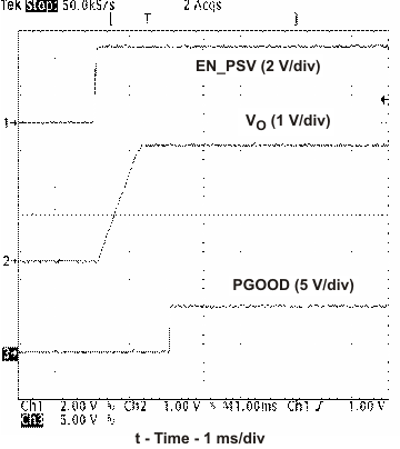
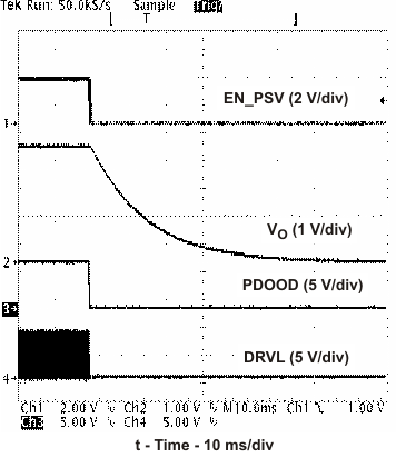
8.3 System Examples
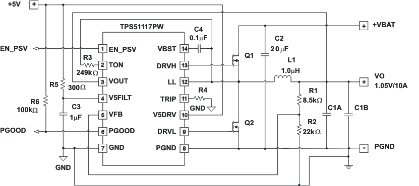 Figure 24. 1.05-V/10-A Application from VBAT (PW Package)
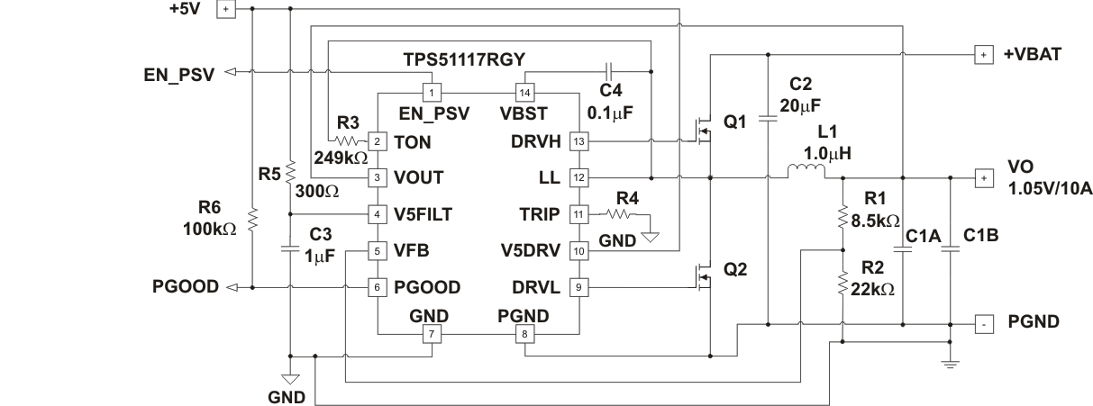 Figure 25. 1.05-V/10-A Application from VBAT (RGY Package)