SLVS616C November 2005 – December 2014 TPS51124
PRODUCTION DATA.
- 1 Features
- 2 Applications
- 3 Description
- 4 Revision History
- 5 Pin Configuration and Functions
- 6 Specifications
- 7 Detailed Description
- 8 Application and Implementation
- 9 Power Supply Recommendations
- 10Layout
- 11Device and Documentation Support
- 12Mechanical, Packaging, and Orderable Information
Package Options
Mechanical Data (Package|Pins)
- RGE|24
Thermal pad, mechanical data (Package|Pins)
- RGE|24
Orderable Information
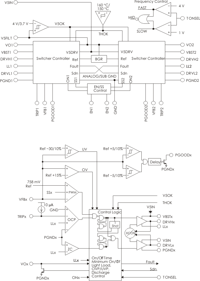
7 Detailed Description
7.1 Overview
The TPS51124 is a cost-effective, dual-synchronous buck controller targeted for notebook I/O and low voltage system bus supply solutions. With D-CAP™ control mode implemented, compensation network can be removed. Besides, the fast transient response also reduced the output capacitance.
7.3 Feature Description
7.3.1 PWM Operation
The main control loop of the switching mode power supply (SMPS) is designed as an adaptive on-time pulse width modulation (PWM) controller. It supports a proprietary D-CAP Mode. D-CAP Mode uses an internal compensation circuit and is suitable for low external component-count configuration, with appropriate amount of ESR at the output capacitor(s). The output voltage is monitored at a feedback point voltage. The reference voltage at the feedback point is a combination of a fixed 0.750-V precision reference and a synchronized, precision 15-mV ramp signal. Lower output voltages in notebook systems (e.g., 1.05 V, 1.5 V) require extremely low output ripple. By providing a ramp signal, the TPS51124 is easier to use in low-output ripple systems. The combination of the precision ramp and reference yield an effective target reference of 0.758 V. The accuracy of this effective reference remains 1.3% over line and temperature.
At the beginning of each cycle, the synchronous high-side MOSFET is turned on, or becomes ON state. This MOSFET is turned off, or becomes OFF state, after the internal one-shot timer expires. This one shot is determined by the converter’s input voltage, VIN, and the output voltage, VOUT, to keep the frequency fairly constant over the input voltage range; hence, it is called adaptive on-time control (see PWM Frequency and Adaptive On-time Control). The high-side MOSFET is turned on again when feedback information indicates insufficient output voltage, and inductor current information indicates a below-the-over-current limit condition. Repeating operation in this manner, the controller regulates the output voltage. The synchronous low-side MOSFET is turned on each OFF state to keep the conduction loss at a minimum. The low-side MOSFET is turned off when the inductor current information detects zero level. This enables seamless transition to the reduced frequency operation at light-load conditions so that high efficiency is kept over a broad range of load current.
7.3.2 Light-Load Condition
TPS51124 automatically reduces switching frequency at light-load conditions to maintain high efficiency. This reduction of frequency is achieved smoothly and without increase of Vout ripple or load regulation. Detail operation is described as follows. As the output current decreases from heavy-load condition, the inductor current is also reduced, and eventually comes to the point that its valley touches zero current, which is the boundary between continuous conduction and discontinuous conduction modes. The low-side MOSFET is turned off when this zero inductor current is detected. As the load current is further decreased, the converter runs in discontinuous conduction mode and it takes longer and longer to discharge the output capacitor to the level that requires the next ON cycle. The ON time is kept the same as that in the heavy-load condition. In reverse, when the output current increases from light load to heavy load, the switching frequency increases to the preset value as the inductor current reaches the continuous conduction. The transition load point to the light-load operation, IOUT(LL) (i.e., the threshold between continuous and discontinuous conduction mode) can be calculated as follows;

where f is the PWM switching frequency.
Switching frequency versus output current in the light-load condition is a function of L, f, Vin, and Vout, but it decreases almost proportional to the output current from the IOUT(LL) given in Equation 1.
It should be noted that in the PWM control path, there is a small ramp. This ramp is transparent in normal, continuous conduction mode and does not measurably affect the regulation voltage. However, in discontinuous, light-load mode, an upward shift in regulation voltage of about 0.75% will be observed. The variation of this shift minimally affects the reference tolerance. Therefore, the reference value in skip mode is 0.764 V ±1.3% over line and temperature.
7.3.3 Low-Side Driver
The low-side driver is designed to drive high current low RDS(on) N-channel MOSFET(s). The drive capability is represented by its internal resistances, which are 4 Ω for V5IN to DRVLx, and 1 Ω for DRVLx to PGNDx. A dead time to prevent shoot through is internally generated between high-side MOSFET off to low-side MOSFET on, and low-side MOSFET off to high-side MOSFET on. A 5-V bias voltage is delivered from V5IN supply. The instantaneous drive current is supplied by an input capacitor connected between V5IN and GND. The average drive current is equal to the gate charge at Vgs = 5 V times switching frequency. This gate drive current, as well as the high-side gate drive current times 5 V, makes the driving power that needs to be dissipated from TPS51124 package.
7.3.4 High-Side Driver
The high-side driver is designed to drive high-current, low RDS(on) N-channel MOSFET(s). When configured as a floating driver, 5-V bias voltage is delivered from V5IN supply. The average drive current is also calculated by the gate charge at Vgs = 5 V times switching frequency. The instantaneous drive current is supplied by the flying capacitor between VBSTx and LLx pins. The drive capability is represented by its internal resistances, which are 5 Ω for VBSTx to DRVHx and 1.5 Ω for DRVHx to LLx.
7.3.5 PWM Frequency and Adaptive On-Time Control
TPS51124 employs adaptive on-time control scheme and does not have a dedicated oscillator on board. However, the part runs with pseudo-constant frequency by feed-forwarding the input and output voltage into the on-time one-shot timer. The frequencies are set by TONSEL terminal connection as Table 1. The on-time is controlled inverse proportional to the input voltage and proportional to the output voltage so that the duty ratio is kept as VOUT/VIN technically with the same cycle time. Although the TPS51124 does not have a pin connected to VIN, the input voltage is monitored at LLx pin during the ON state. This helps pin count reduction to make the part compact without sacrificing its performance.
Table 1. TONSEL Connection and Switching Frequency Table
(Frequencies Are Approximate)
| TONSEL CONNECTION | SWITCHING FREQUENCY | |
|---|---|---|
| CH1 | CH2 | |
| GND | 240 kHz | 300 kHz |
| FLOAT (Open) | 300 kHz | 360 kHz |
| V5FILT | 360 kHz | 420 kHz |
7.3.6 Powergood
The TPS51124 has the powergood output for both switcher channels. The powergood function is activated after soft start has finished. If the output voltage becomes within ±5% of the target value, internal comparators detect power good state and the power good signal becomes high after a 510-μs internal delay. During start-up, this internal delay starts after 1.7 times internal soft-start time to avoid a glitch of powergood signal. If the feedback voltage goes outside of ±10% of the target value, the powergood signal becomes low after 10-μs internal delay.
Also note that if the feedback voltage goes +10% above target value and the powergood signal flags low, then the loop attempts to correct the output by turning on the low-side driver (forced PWM mode). After the feedback voltage returns to be within +5% of the target value and the powergood signal goes high, the controller returns back to auto-skip mode.
7.3.7 Output Discharge Control
TPS51124 discharges the output when ENx is low, or the controller is turned off by the protection functions (OVP, UVP, UVLO, and thermal shutdown). TPS51124 discharges outputs using an internal, 10-Ω MOSFET which is connected to VOx and PGNDx. The external low-side MOSFET is not turned on for the output discharge operation to avoid the possibility of causing negative voltage at the output. Output discharge time constant is a function of the output capacitance and the resistance of the internal discharge MOSFET. This discharge ensures that, on restart, the regulated voltage always starts from zero volts. In case a SMPS is restarted before discharge completion, discharge is terminated and the switching resumes after the reference level, ramped up by an internal DAC, comes back to the remaining output voltage.
7.3.8 Current Protection
TPS51124 has cycle-by-cycle over-current limiting control. The inductor current is monitored during the OFF state and the controller keeps the OFF state during the inductor current is larger than the over-current trip level. In order to provide both good accuracy and cost effective solution, TPS51124 supports temperature compensated MOSFET RDS(on) sensing. TRIPx pin should be connected to GND through the trip voltage setting resistor, Rtrip. TRIPx terminal sources 10-μA Itrip current and the trip level is set to the OCL trip voltage Vtrip as below.

The trip level should be in the range of 30 mV to 200 mV over all operational temperatures. The inductor current is monitored by the voltage between PGNDx pin and LLx pin so that LLx pin should be connected to the drain terminal of the low-side MOSFET. Itrip has 4200 ppm/°C temperature slope to compensate the temperature dependency of the RDS(on). PGNDx is used as the positive current sensing node so that PGNDx should be connected to the source terminal of the low-side MOSFET. As the comparison is done during the OFF state, Vtrip sets the valley level of the inductor current. Thus, the load current at over-current threshold, Iocl, can be calculated as follows;

In an over-current condition, the current to the load exceeds the current to the output capacitor; thus, the output voltage tends to fall off (droop). Eventually, it ends up crossing the under-voltage protection threshold and shuts down.
7.3.9 Over and Undervoltage Protection
TPS51124 monitors a resistor divided feedback voltage to detect over and under voltage. When the feedback voltage becomes higher than 115% of the target voltage, the OVP comparator output goes high and the circuit latches as the high-side MOSFET driver OFF and the low-side MOSFET driver ON.
Also, the TPS51124 monitors VOx voltage directly and if it becomes greater than 5.75 V, the TPS51124 turns off the top MOSFET driver, and shuts off both drivers of the other channel.
When the feedback voltage becomes lower than 70% of the target voltage, the UVP comparator output goes high and an internal UVP delay counter begins counting. After 32 μs, TPS51124 latches OFF both top and bottom MOSFET drivers, and shuts off both drivers of the other channel. This function is enabled after 1.7 times soft-start delay time, approximately 2 ms, to ensure start-up properly.
7.3.10 UVLO Protection
TPS51124 has V5FILT under-voltage lock-out protection (UVLO). When the V5FILT voltage is lower than UVLO threshold voltage, the TPS51124 is shut off. This is non-latch protection.
7.3.11 Thermal Shutdown
TPS51124 monitors its own temperature. If the temperature exceeds the threshold value (typically 160°C), the switchers are shut off as both DRVH and DRVL at low; the output discharge function is enabled. TPS51124 is shut off. This is non-latch protection.
7.4 Device Functional Modes
7.4.1 Enable and Soft-Start
The TPS51124 has dedicated ENx pin to enable/disable each channel. When the ENx pin is low, the corresponding channel is disabled; When the ENx pin becomes high, an internal 1.2-ms, voltage servo begins ramping up the reference voltage to the PWM comparator, the output voltage of corresponding channel will ramp up accordingly. By this mean, smooth control of the output voltage is maintained during start-up.
As TPS51124 shares one voltage servo with both channels, if ENx pin is set to high while another channel is starting up, soft start is postponed until another channel soft start has completed. If both of EN1 and EN2 are set high at a same time, both channels start up at same time.