SLVS616C November 2005 – December 2014 TPS51124
PRODUCTION DATA.
- 1 Features
- 2 Applications
- 3 Description
- 4 Revision History
- 5 Pin Configuration and Functions
- 6 Specifications
- 7 Detailed Description
- 8 Application and Implementation
- 9 Power Supply Recommendations
- 10Layout
- 11Device and Documentation Support
- 12Mechanical, Packaging, and Orderable Information
Package Options
Mechanical Data (Package|Pins)
- RGE|24
Thermal pad, mechanical data (Package|Pins)
- RGE|24
Orderable Information
5 Pin Configuration and Functions
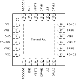
Pin Functions
| PIN | I/O | DESCRIPTION | |
|---|---|---|---|
| NAME | NO. | ||
| DRVH1 | 21 | O | Synchronous high-side MOSFET driver outputs. LL node referenced floating drivers. The gate drive voltage is defined by the voltage across VBST to LL node flying capacitor. |
| DRVH2 | 10 | ||
| DRVL1 | 19 | O | Synchronous low-side MOSFET driver outputs. PGND referenced drivers. The gate-drive voltage is defined by V5IN voltage. |
| DRVL2 | 12 | ||
| EN1 | 23 | I | Channel 1 and channel 2 enable pins. Connect to 5 V or 3.3 V to turn on SMPS |
| EN2 | 8 | ||
| GND | 3 | I | Signal ground pin |
| LL1 | 20 | I/O | Switch node connections for high-side drivers return. Also serve as input to current comparators and input voltage monitor for on-time control circuitry. |
| LL2 | 11 | ||
| PGND1 | 18 | I/O | Ground returns for DRVL1 and DRVL2. Also serve as input of current comparators. Connect PGND1, PGND2, and GND strongly together near the IC. Output discharge current flows through this pin, also. |
| PGND2 | 13 | ||
| PGOOD1 | 24 | O | Power Good window comparator open drain output for channel 1 and 2. Pull up with a resistor to 5 V, or appropriate signal voltage. Current capability is 5 mA. PGOOD goes high 0.5 ms after VFB comes within specified limits. Power bad, or the terminal goes low, is within 10 μs. |
| PGOOD2 | 7 | ||
| TONSEL | 4 | I | On-time selection pin. See Table 1. |
| TRIP1 | 17 | I | Overcurrent trip point set input. Connect resistor from this pin to GND to set threshold for synchronous low-side RDS(on) sense. Voltage across this pin and GND is compared to voltage across PGND and LL at over-current comparator. |
| TRIP2 | 14 | ||
| VBST1 | 22 | I | Supply input for synchronous high-side MOSFET driver (Boost Terminal). Connect capacitor from this pin to respective LL terminals. An internal PN diode is connected between V5IN to each of these pins. User can add external Schottky diode if forward drop is critical to drive the MOSFET. |
| VBST2 | 9 | ||
| VFB1 | 2 | I | SMPS voltage feedback inputs. Connect with feedback resistor divider. |
| VFB2 | 5 | ||
| VO1 | 1 | I | Output connections to SMPS. These terminals serve two functions: On-time adjustment and output discharge. |
| VO2 | 6 | ||
| V5FILT | 15 | I | 5-V power supply input for the entire control circuit except the MOSFET drivers. Connect RC low-pass filter from V5IN to V5FILT. |
| V5IN | 16 | I | 5-V power supply input for FET gate drivers. Internally connected to VBSTx by PN diodes. |