SLVSCT3 March 2015 TPS51275B-1
PRODUCTION DATA.
- 1 Features
- 2 Applications
- 3 Description
- 4 Typical Application Diagram
- 5 Revision History
- 6 Pin Configuration and Functions
- 7 Specifications
-
8 Detailed Description
- 8.1 Overview
- 8.2 Functional Block Diagram
- 8.3
Feature Description
- 8.3.1 PWM Operations
- 8.3.2 Adaptive On-Time and PWM Frequency Control
- 8.3.3 Light-Load Condition in Out-of-Audio Operation
- 8.3.4 Enable and Power Good
- 8.3.5 Soft-Start and Discharge
- 8.3.6 VREG5 and VREG3 Linear Regulators
- 8.3.7 VCLK for Charge Pump
- 8.3.8 Overcurrent Protection
- 8.3.9 Output Overvoltage and Undervoltage Protection
- 8.3.10 Undervoltage Lockout Protection
- 8.3.11 Over-Temperature Protection (OTP)
- 8.4 Device Functional Modes
- 9 Application and Implementation
- 10Power Supply Recommendations
- 11Layout
- 12Device and Documentation Support
- 13Mechanical, Packaging, and Orderable Information
Package Options
Mechanical Data (Package|Pins)
- RUK|20
Thermal pad, mechanical data (Package|Pins)
- RUK|20
Orderable Information
11 Layout
11.1 Layout Guidelines
Good layout is essential for stable power-supply operation. Follow these guidelines for an efficient PCB layout.
11.1.1 Placement
- Place voltage setting resistors close to the device pins.
- Place bypass capacitors for the VREG5 and VREG3 regulators close to the device pins.
11.1.2 Routing (Sensitive Analog Portion)
- Use small copper space for the VFBx pins. Short and narrow traces are available to avoid noise coupling.
- Connect the VFB resistor trace to the positive node of the output capacitor. Routing the inner layer away from power traces is recommended.
- Use short and wide trace from the VFB resistor to vias to GND (internal GND plane).
11.1.3 Routing (Power portion)
- Use wider and shorter traces of the DRVLx pin for the low-side gate drivers to reduce stray inductance.
- Use the parallel traces of the SWx and DRVHx pins for the high-side MOSFET gate drive in a same layer or on adjoin layers, and keep these traces away from the DRVLx pin.
- Use wider and shorter traces between the source terminal of the high-side MOSFET and the drain terminal of the low-side MOSFET
- The thermal pad is the GND terminal of this device. Five or more vias with 0.33-mm (13-mils) diameter connected from the thermal pad to the internal GND plane should be used to have strong GND connection and help heat dissipation.
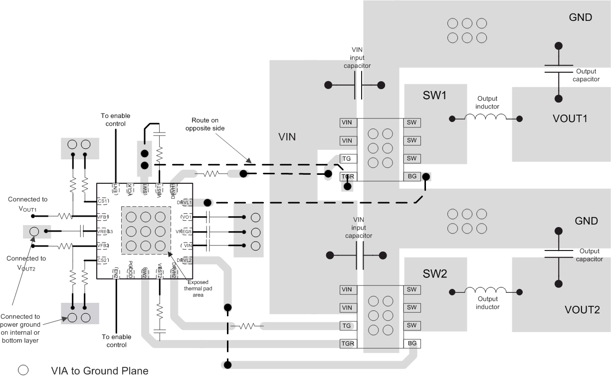
11.2 Layout Example
 Figure 26. TPS51275B-Q1 Layout Example