SLUS909B May 2009 – August 2014 TPS53126
PRODUCTION DATA.
- 1 Features
- 2 Applications
- 3 Description
- 4 Simplified Schematics
- 5 Revision History
- 6 Pin Configurations and Functions
- 7 Specifications
-
8 Detailed Description
- 8.1 Overview
- 8.2 Functional Block Diagram
- 8.3
Feature Description
- 8.3.1 PWM Operation
- 8.3.2 Drivers
- 8.3.3 PWM Frequency And Adaptive On-time Control
- 8.3.4 5 Volt Regulator
- 8.3.5 Soft Start
- 8.3.6 Pre-Bias Support
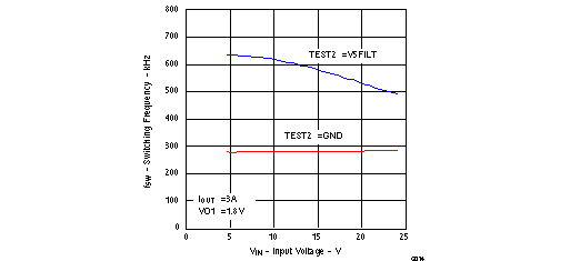
- 8.3.7 Switching Frequency Selection
- 8.3.8 Output Discharge Control
- 8.3.9 Overcurrent Limit
- 8.3.10 Over/under Voltage Protection
- 8.3.11 UVLO Protection
- 8.3.12 Thermal Shutdown
- 8.4 Device Functional Modes
- 9 Application and Implementation
- 10Power Supply Recommendations
- 11Layout
- 12Device and Documentation Support
- 13Mechanical, Packaging, and Orderable Information
Package Options
Refer to the PDF data sheet for device specific package drawings
Mechanical Data (Package|Pins)
- RGE|24
- PW|24
Thermal pad, mechanical data (Package|Pins)
- RGE|24
Orderable Information
9 Application and Implementation
9.1 Application Information
9.2 350 kHz Operation Application
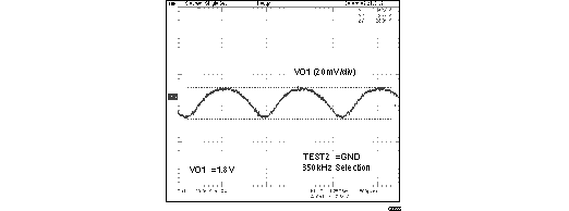
The schematic of Figure 14 shows a typical 350 kHz application schematic. The 350 kHz switching frequency is selected by connecting TEST2 to the GND pin. The input voltage is 4.5 V to 24 V and the output voltage is 1.8 V for VO1 and 1.05 V for VO2.
 Figure 14. Typical Application Circuit at 350kHz Switching Frequency Selection (TEST2 Pin = GND)
9.2.1 Design Requirements
Table 1. Design Parameters
| PARAMETERS | CHANNEL 1 | CHANNEL 2 |
|---|---|---|
| Input voltage | 4.5 V to 24 V | 4.5 V to 24 V |
| Output voltage | 1.8 V | 1.05 V |
| Output Current | 4 A | 4 A |
| Switching Frequency | 350 kHz | 350 kHz |
9.2.2 Detailed Design Procedure
9.2.2.1 Choose Inductor
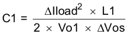
The inductance value is selected to provide approximately 30% peak to peak ripple current at maximum load. Larger ripple current increases output ripple voltage, improve S/N ratio and contribute to stable operation. Equation 3 can be used to calculate L1.
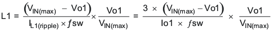
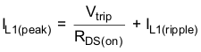
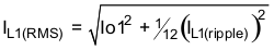
The inductors current ratings needs to support both the RMS (thermal) current and the Peak (saturation) current. The RMS and peak inductor current can be estimated as follows:
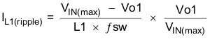
Note: The calculation above shall serve as a general reference. To further improve transient response, the output inductance could be reduced further. This needs to be considered along with the selection of the output capacitor.
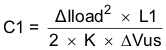
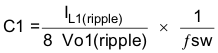
9.2.2.2 Choose Output Capacitor
The capacitor value and ESR determines the amount of output voltage ripple and load transient response. Recommend to use ceramic output capacitor.
Where:
Select the capacitance value greater than the largest value calculated from Equation 7, Equation 8 and Equation 10. The capacitance for C1 should be greater than 66 μF.
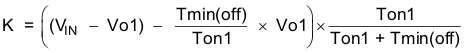
Where:
ΔVos = the allowable amount of overshoot voltage in load transition
ΔVus = the allowable amount of undershoot voltage in load transition
Tmin(off) = Min-off time
9.2.2.3 Choose Input Capacitor
The TPS53126 requires an input decoupling capacitor and a bulk capacitor is needed depending on the application. A minimum 10-μF high-quality ceramic capacitor is recommended for the input capacitor. The capacitor voltage rating needs to be greater than the maximum input voltage.
9.2.2.4 Choose Bootstrap Capacitor
The TPS53126 requires a bootstrap capacitor from SWx to VBSTx to provide the floating supply for the high-side drivers. A minimum 0.1-μF high-quality ceramic capacitor is recommended. The voltage rating should be greater than 6 V.
9.2.2.5 Choose VREG5 and V5FILT Capacitors
The TPS53126 requires both the VREG5 regulator and V5FILT input are bypassed. A minimum 4.7-μF high-quality ceramic capacitor must be connected between the VREG5 and GND for proper operation. A minimum 1.0-μF high-quality ceramic capacitor must be connected between the V5FILT and GND for proper operation. Both of these capacitors’ voltage ratings should be greater than 6 V.
9.2.2.6 Choose Output Voltage Set Point Resistors
The output voltage is set with a resistor divider from output voltage node to the VFBx pin. It is recommended to use 1% tolerance or better resisters. Select R2 between 10 kΩ and 100 kΩ and use Equation 11 and Equation 12 to calculate R1.
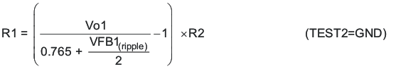
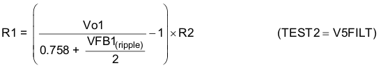
Where:
VFB1(ripple) = Ripple Voltage at VFB1
9.2.3 350 kHz Application Curves
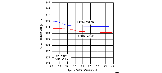
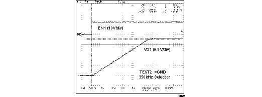
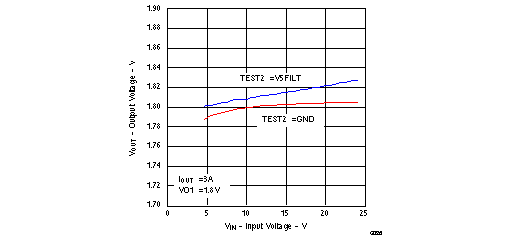
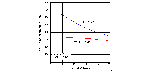
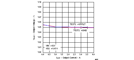
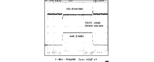
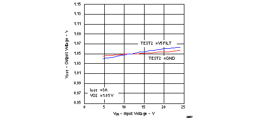
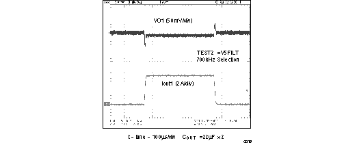
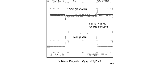
Application curves Figure 15, Figure 16, Figure 17, Figure 18, Figure 23 and Figure 24 apply to both the circuits of 350 kHz Operation Application and 700 Khz Operation Application.
| IO1 = 3 A |
| VIN = 12 V |
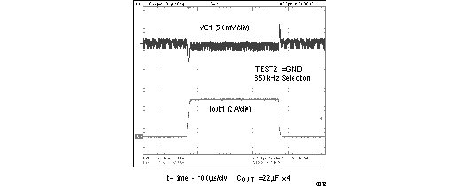
| CH1, TEST2 = GND |
| IO = 3 A |
| IO2 = 3 A |
| VIN = 12 V |
| CH2, TEST2 = GND |
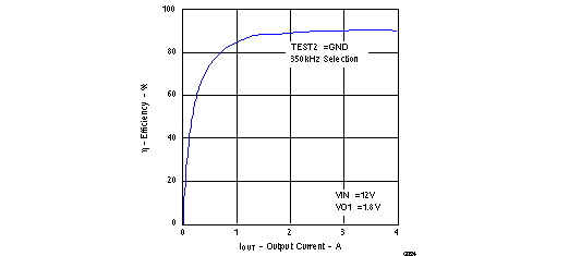
| VIN = 12 V |
| IO = 3 A |
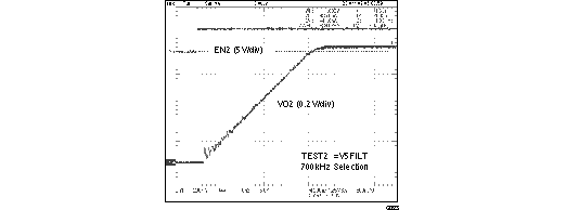
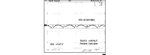
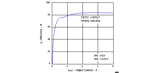
9.3 700 Khz Operation Application
The schematic of Figure 26 shows a typical 700 kHz application schematic. The 700 kHz switching frequency is selected by connecting TEST2 to the V5FILT pin. The input voltage is 4.5 V to 24 V and the output voltage is 1.8 V for VO1 and 1.05 V for VO2.
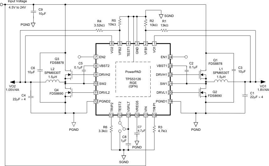 Figure 26. Typical Application Circuit at 700 kHz Switching frequency Selection (TEST2 Pin = V5FILT)
9.3.1 Design Parameters
9.3.2 Detailed Design Procedure
For the Detailed Design Procedure, refer to Detailed Design Procedure.
700 kHz Application Curves
Application curves Figure 15, Figure 16, Figure 17, Figure 18, Figure 23 and Figure 24 apply to both the circuits of 350 kHz Operation Application and 700 Khz Operation Application.
| CH1, TEST2 = V5FILT |
| CH2, TEST2 = V5FILT |
| VIN = 12 V |