SLUS909B May 2009 – August 2014 TPS53126
PRODUCTION DATA.
- 1 Features
- 2 Applications
- 3 Description
- 4 Simplified Schematics
- 5 Revision History
- 6 Pin Configurations and Functions
- 7 Specifications
-
8 Detailed Description
- 8.1 Overview
- 8.2 Functional Block Diagram
- 8.3
Feature Description
- 8.3.1 PWM Operation
- 8.3.2 Drivers
- 8.3.3 PWM Frequency And Adaptive On-time Control
- 8.3.4 5 Volt Regulator
- 8.3.5 Soft Start
- 8.3.6 Pre-Bias Support
- 8.3.7 Switching Frequency Selection
- 8.3.8 Output Discharge Control
- 8.3.9 Overcurrent Limit
- 8.3.10 Over/under Voltage Protection
- 8.3.11 UVLO Protection
- 8.3.12 Thermal Shutdown
- 8.4 Device Functional Modes
- 9 Application and Implementation
- 10Power Supply Recommendations
- 11Layout
- 12Device and Documentation Support
- 13Mechanical, Packaging, and Orderable Information
Package Options
Refer to the PDF data sheet for device specific package drawings
Mechanical Data (Package|Pins)
- RGE|24
- PW|24
Thermal pad, mechanical data (Package|Pins)
- RGE|24
Orderable Information
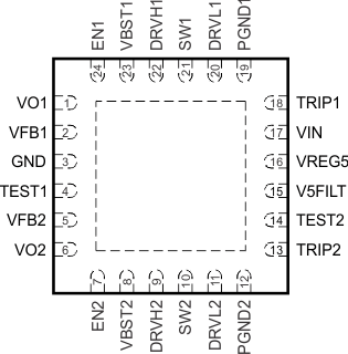
6 Pin Configurations and Functions
24 Pin VQFN
RGE Package
(Top View)
24 Pin TSSOP
PW Package
(Top View)
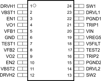
Pin Functions
| PIN | I/O | DESCRIPTION | ||
|---|---|---|---|---|
| NAME | VQFN 24 NUMBER |
TSSOP 24 NUMBER |
||
| VBST1, VBST2 | 23, 8 | 2, 11 | I | Supply input for high-side NFET driver (Boost Terminal). Bypass to SWx with a high-quality 0.1μF ceramic capacitor. An external schottky diode can be added if forward drop is critical to drive the high-side FET. |
| EN1, EN2 | 24, 7 | 3, 10 | I | Channel 1 and channel 2 high level enable pins. |
| VO1, VO2 | 1, 6 | 4, 9 | I | Output voltage inputs for on-time adjustment and output discharge. Connect directly to the output voltage. |
| VFB1, VFB2 | 2, 5 | 5, 8 | I | D-CAP2 feedback inputs. Connect to output voltage with resistor divider. |
| GND | 3 | 6 | I | Signal ground pin. Connect to PGND1, PGND2 and system ground at a single point. |
| DRVH1, DRVH2 | 22, 9 | 1, 12 | O | High-side MOSFET gate driver outputs. SWx referenced drivers switch between SWx (OFF) and VBSTx (ON). |
| SW1, SW2 | 21, 10 | 24, 13 | I/O | Switch node connections for both the high-side drivers and the current comparators. |
| DRVL1, DRVL2 | 20, 11 | 23, 14 | O | Low-side MOSFET gate driver outputs. PGND referenced drivers switch between PGNDx (OFF) and VREG5 (ON). |
| PGND1, PGND2 | 19, 12 | 22, 15 | I/O | Power ground connections for both the low-side drivers and the current comparators. Connect PGND1, PGND2 and GND strongly together near the IC. |
| TRIP1, TRIP2 | 18, 13 | 21, 16 | I | Over current trip point programming pin. Connect to GND with a resistor to GND to set threshold for low-side RDS(on) current limit. |
| VIN | 17 | 20 | I | Supply Input for 5V linear regulator. |
| V5FILT | 15 | 18 | I | 5V supply input for the entire control circuit except the MOSFET drivers. Bypass to GND with a minimum 1.0μF, high-quality ceramic capacitor. V5FILT is connected to VREG5 via an internal 10Ω resistor. |
| VREG5 | 16 | 19 | O | Output of 5V linear regulator and supply for MOSFET drivers. Bypass to GND with a minimum 4.7μF high-quality ceramic capacitor. VREG5 is connected to V5FILT via an internal 10Ω resistor. |
| TEST1 | 4 | 7 | O | Test interface pin, not used during application. Connect directly to GND. |
| TEST2 | 14 | 17 | I | Frequency select pin. Connect to GND for 350kHz switching. Connect to V5FILT for 700kHz switching. |