SLVSA93A March 2010 – August 2014 TPS53127
PRODUCTION DATA.
- 1 Features
- 2 Applications
- 3 Description
- 4 Simplified Schematic
- 5 Revision History
- 6 Pin Configuration and Functions
- 7 Specifications
- 8 Detailed Description
- 9 Application and Implementation
- 10Power Supply Recommendations
- 11Layout
- 12Device and Documentation Support
- 13Mechanical, Packaging, and Orderable Information
Package Options
Mechanical Data (Package|Pins)
Thermal pad, mechanical data (Package|Pins)
- RGE|24
Orderable Information
9 Application and Implementation
9.1 Application Information
9.2 Typical Application, QFN
The TPS53127 is a Dual D-CAP2™ Mode Control Step-Down Controller in a realistic cost-sensitive application. Providing both a low core-type 1.05 V and I/O type 1.8 V output from a loosely regulated 12 V source. Idea applications are: Digital TV Power Supply, Networking Home Pin, Digital Set-Top Box (STB), DVD Player/Recorder, and Gaming Consoles.
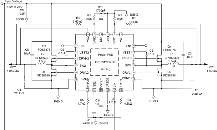 Figure 12. Typical Application Circuit
9.2.1 Design Requirements (QFN)
Table 1. Design Parameters
| PARAMETERS | EXAMPLE VALUES |
|---|---|
| Input voltage | 12 V |
| Output voltage | VO1 = 1.8 V, VO2 = 1.05 V |
9.2.2 Detailed Design Procedure (QFN)
9.2.2.1 Choose Inductor
The inductance value is selected to provide approximately 30% peak to peak ripple current at maximum load. Larger ripple current increases output ripple voltage, improve S/N ratio and contribute to stable operation.
Equation 3 can be used to calculate L1.
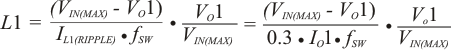
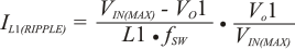
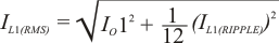
The inductors current ratings needs to support both the RMS (thermal) current and the Peak (saturation) current. The RMS and peak inductor current can be estimated as follows.
Note: The calculation above shall serve as a general reference. To further improve transient response, the output inductance could be reduced further. This needs to be considered along with the selection of the output capacitor.
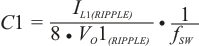
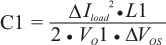
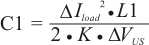
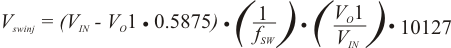
9.2.2.2 Choose Output Capacitor
The capacitor value and ESR determines the amount of output voltage ripple and load transient response. it is recommended to use a ceramic output capacitor.
Where
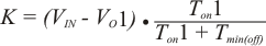
Select the capacitance value greater than the largest value calculated from Equation 7, Equation 8 and Equation 9. The capacitance for C1 should be greater than 66 μF.
Where
- ΔVOS = The allowable amount of overshoot voltage in load transition.
- ΔVUS = The allowable amount of undershoot voltage in load transition.
- tmin(off) = Minimum off time
9.2.2.3 Choose Input Capacitor
The TPS53127 requires an input decoupling capacitor and a bulk capacitor is needed depending on the application. A minimum 10-μF high-quality ceramic capacitor is recommended for the input capacitor. The capacitor voltage rating needs to be greater than the maximum input voltage.
9.2.2.4 Choose Bootstrap Capacitor
The TPS53127 requires a bootstrap capacitor from SW to VBST to provide the floating supply for the high-side drivers. A minimum 0.1-μF high-quality ceramic capacitor is recommended. The voltage rating should be greater than 10 V.
9.2.2.5 Choose VREG5 and V5FILT Capacitor
The TPS53127 requires both the VREG5 regulator and V5FILT input are bypassed. A minimum 4.7-μF high-quality ceramic capacitor must be connected between the VREG5 and GND for proper operation. A minimum 1-μF high-quality ceramic capacitor must be connected between the V5FILT and GND for proper operation. Both of these capacitors’ voltage ratings should be greater than 10 V.
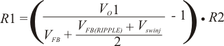
9.2.2.6 Choose Output Voltage Set Point Resistors
The output voltage is set with a resistor divider from the output voltage node to the VFBx pin. It is recommended to use 1% tolerance or better resisters. Select R2 between 10 kΩ and 100 kΩ and use Equation 11 or Equation 12 to calculate R1.
Where
VFB(RIPPLE) = Ripple voltage at VFB
Vswinj = Ripple voltage at error comparator
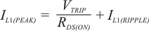
9.2.2.7 Choose Over Current Set Point Resistor
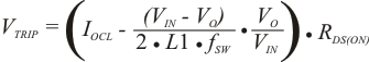
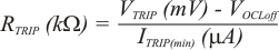
Where:
- RDS(ON) = Low side FET on-resistance
- ITRIP(min) = TRIP pin source current (8.5 μA)
- VOCL0ff = Minimum over current limit offset voltage (–20 mV)
- IOCL = Over current limit
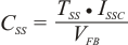
9.2.2.8 Choose Soft Start Capacitor
Soft start time equation is as follows.
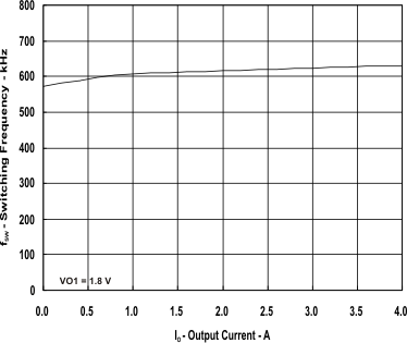
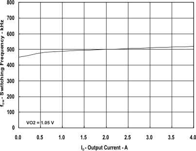
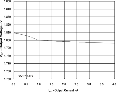
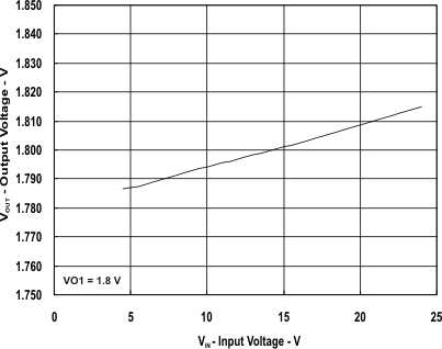
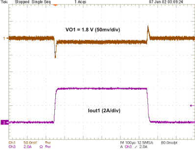
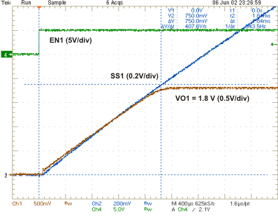
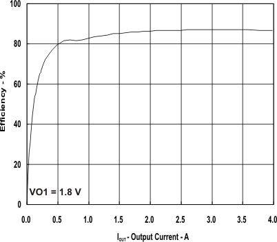
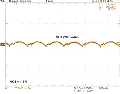
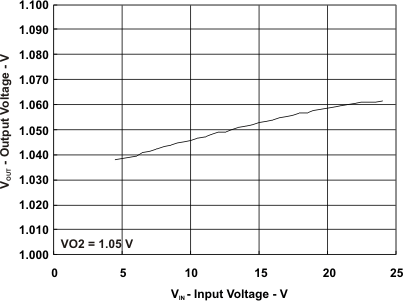
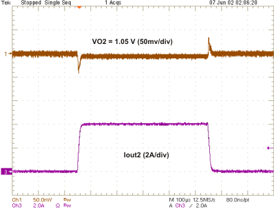
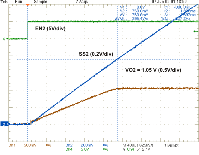
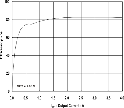
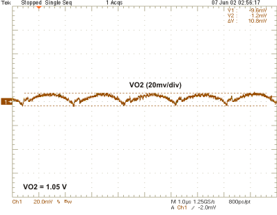
9.2.3 Application Curves (QFN)

9.3 Typical Application Circuit, TSSOP
The TPS53127is a Dual D-CAP2™ Mode Control Step-Down Controller in a realistic cost-sensitive application. Providing both a low core-type 1.05 V and I/O type 1.8V output from a loosely regulated 12 V source.
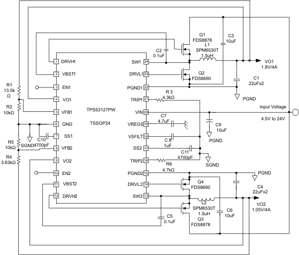 Figure 27. Typical Application Circuit
9.3.1 Design Requirements
For the Design Requirements, refer to Design Requirements (QFN).
9.3.2 Detailed Design Procedure
For the Detailed Design Procedure, refer to Detailed Design Procedure (QFN).
9.3.3 Application Curves
For the Application Curves, refer to Application Curves (QFN).