SLVSA93A March 2010 – August 2014 TPS53127
PRODUCTION DATA.
- 1 Features
- 2 Applications
- 3 Description
- 4 Simplified Schematic
- 5 Revision History
- 6 Pin Configuration and Functions
- 7 Specifications
- 8 Detailed Description
- 9 Application and Implementation
- 10Power Supply Recommendations
- 11Layout
- 12Device and Documentation Support
- 13Mechanical, Packaging, and Orderable Information
Package Options
Mechanical Data (Package|Pins)
Thermal pad, mechanical data (Package|Pins)
- RGE|24
Orderable Information
7 Specifications
7.1 Absolute Maximum Ratings
over operating free-air temperature range (unless otherwise noted) (1)(1) Stresses beyond those listed under "absolute maximum ratings" may cause permanent damage to the device. These are stress ratings only and functional operation of the device at these or any other conditions beyond those indicated under "recommended operating conditions" are not implied. Exposure to absolute-maximum-rated conditions for extended periods may affect device reliability.
7.2 Handling Ratings
| MIN | MAX | UNIT | |||
|---|---|---|---|---|---|
| TSTG | Storage temperature range | –55 | 150 | °C | |
| V(ESD) | Electrostatic discharge | Human body model (HBM), per AN/ESDA/JEDEC JS-001, all pins(1) | –2000 | 2000 | V |
| Charged device model (CDM), per JEDEC specification JESD22-C101, all pins(2) | –500 | 500 | V | ||
(1) JEDEC document JEP155 states that 500-V HBM allows safe manufacturing with a standard ESD control process.
(2) JEDEC document JEP157 states that 250-V CDM allows safe manufacturing with a standard ESD control process
7.3 Recommended Operating Conditions
over operating free-air temperature range (unless otherwise noted)7.4 Thermal Information
| THERMAL METRIC(1) | TPS53127 | UNIT | ||
|---|---|---|---|---|
| PW 24 PINS | RGE 24 PINS | |||
| RθJA | Junction-to-ambient thermal resistance | 88.9 | 35.4 | °C/W |
| RθJC(top) | Junction-to-case (top) thermal resistance | 26.5 | 39.1 | |
| RθJB | Junction-to-board thermal resistance | 43.5 | 13.6 | |
| ψJT | Junction-to-top characterization parameter | 1.1 | 0.5 | |
| ψJB | Junction-to-board characterization parameter | 43.0 | 13.6 | |
| RθJC(bot) | Junction-to-case (bottom) thermal resistance | n/a | 3.8 | |
(1) For more information about traditional and new thermal metrics, see the IC Package Thermal Metrics application report, SPRA953.
7.5 Electrical Characteristics
over operating free-air temperature range (unless otherwise noted)| PARAMETER | TEST CONDITIONS | MIN | TYP | MAX | UNIT | |
|---|---|---|---|---|---|---|
| SUPPLY CURRENT | ||||||
| IIN | VIN supply current | VIN current, TA = 25°C, VREG5 tied to V5FILT, EN1 = EN2 = 5 V, VFB1 = VFB2 = 0.8 V, SW1 = SW2 = 0.5 V |
450 | 800 | μA | |
| I(VINSDN) | VIN shutdown current | VIN current, TA = 25°C, no load , EN1 = EN2 = 0 V, VREG5 = ON |
30 | 60 | μA | |
| VFB VOLTAGE AND DISCHARGE RESISTANCE | ||||||
| VBG | Bandgap initial regulation accuracy | TA = 25°C | –1 | 1 | % | |
| V(VFBTHx) | VFBx threshold voltage | TA = 25°C, SWinj = OFF | 748 | 758 | 768 | mV |
| TA = 0°C to 70°C, SWinj = OFF(1) |
746.6 | 769.4 | ||||
| TA = -40°C to 85°C, SWinj = OFF (1) |
745 | 771 | ||||
| I(VFB) | VFB input current | VFBx = 0.8 V, TA = 25°C | –100 | –10 | 100 | nA |
| R(Dischg) | VO discharge resistancee | ENx = 0 V, VOx = 0.5 V, TA = 25°C | 40 | 80 | Ω | |
| VREG5 OUTPUT | ||||||
| V(VREG)5 | VREG5 output voltage | TA = 25°C, 5.5 V < VIN < 24 V, 0 < I(VREG5) < 10 mA |
4.6 | 5.0 | 5.2 | V |
| V(LN5) | Line regulation | 5.5 V < VIN < 24 V, I(VREG5) = 10 mA | 20 | mV | ||
| V(LD5) | Load regulation | 1 mA < I(VREG5) < 10 mA | 40 | mV | ||
| I(VREG5) | Output current | VIN = 5.5 V, V(REG5) = 4.0 V, TA = 25°C |
170 | mA | ||
| OUTPUT: N-CHANNEL MOSFET GATE DRIVERS | ||||||
| R(DRVH) | DRVH resistance | Source, I(DRVHx) = –100 mA | 5.5 | 11 | Ω | |
| Sink, I(DRVHx) = 100 mA | 2.5 | 5 | ||||
| R(DRVL) | DRVL resistance | Source, I(DRVLx) = –100 mA | 4 | 12 | Ω | |
| Sink, I(DRVLx) = 100 mA | 2 | 4 | ||||
| INTERNAL BOOST DIODE | ||||||
| V(FBST) | Forward voltage | V(VREG5-VBSTx), IF = 10 mA, TA = 25°C |
0.7 | 0.8 | 0.9 | V |
| I(VBSTLK) | VBST leakage current | VBSTx = 29 V, SWx = 24 V, TA = 25°C |
0.1 | 1 | μA | |
| SOFT START | ||||||
| I(SSC) | SS1/SS2 charge current | VSS1/VSS2 = 0 V, TA = 25°C | –2.5 | –2 | –1.5 | μA |
| TC(ISSC) | ISSC temperature coefficient | On the basis of 25°C(1) | –4 | 3 | nA/°C | |
| ISSD | SS1/SS2 discharge current | VSS1/VSS2 = 0.5 V | 100 | 150 | μA | |
| UVLO | ||||||
| V(UV5VFILT) | V5FILT UVLO threshold | Wake up | 3.7 | 4.0 | 4.3 | V |
| Hysteresis | 0.2 | 0.3 | 0.4 | |||
| LOGIC THRESHOLD | ||||||
| V(ENH) | ENx high-level input voltage | EN 1/2 | 2.0 | V | ||
| V(ENL) | ENx low-level input voltage | EN 1/2 | 0.3 | V | ||
| CURRENT SENSE | ||||||
| I(TRIP) | TRIP source current | V(TRIPx) = 0.1 V, TA = 25°C | 8.5 | 10 | 11.5 | μA |
| TC(ITRIP) | ITRIP temperature coefficient | On the basis of 25°C | 4000 | ppm/°C | ||
| VOC(Loff) | OCP compensation offset | (V(TRIPx-GND) - V(PGNDx-SWx)) voltage, V(TRIPx-GND) = 60 mV, TA = 25°C |
–15 | 0 | 15 | mV |
| (V(TRIPx-GND) - V(PGNDx-SWx)) voltage, V(TRIPx-GND) = 60 mV |
–20 | 20 | ||||
| VR(trip) | Current limit threshold setting range | V(TRIPx-GND) voltage | 30 | 300 | mV | |
| OUTPUT UNDERVOLTAGE AND OVERVOLTAGE PROTECTION | ||||||
| VOVP | Output OVP trip threshold | OVP detect | 110 | 115 | 120 | % |
| VUVP | Output UVP trip threshold | UVP detect | 65 | 70 | 75 | % |
| Hysteresis (recover < 20 μs) | 10 | |||||
| THERMAL SHUTDOWN | ||||||
| TSDN | Thermal shutdown threshold | Shutdown temperature (1) | 150 | °C | ||
| Hysteresis (1) | 20 | |||||
(1) Not production tested - specified by design.
7.6 Timing Requirements
| MIN | TYP | MAX | UNIT | |||
|---|---|---|---|---|---|---|
| OUTPUT: N-CHANNEL MOSFET GATE DRIVERS | ||||||
| tD | Dead time | DRVHx-low to DRVLx-on | 20 | 50 | 80 | ns |
| DRVLx-low to DRVHx-on | 20 | 40 | 80 | ns | ||
| OUTPUT UNDERVOLTAGE AND OVERVOLTAGE PROTECTION | ||||||
| tOVPDEL | Output OVP prop delay | 1.5 | µs | |||
| tUVPDEL | Output UVP delay | 17 | 30 | 40 | µs | |
| tUVPEN | Output UVP enable delay | UVP enable delay / soft-start time | x1.4 | x1.7 | x2.0 | ms |
7.7 Switching Characteristics
over operating free-air temperature range (unless otherwise noted)| MIN | TYP | MAX | UNIT | |||
|---|---|---|---|---|---|---|
| ON-TIME TIMER CONTROL | ||||||
| tON1L | CH1 on time | SW1 = 12 V, VO1 = 1.8 V | 165 | ns | ||
| tON2L | CH2 on time | SW2 = 12 V, VO2 = 1.8 V | 140 | ns | ||
| tOFF1L | CH1 min off time | SW1 = 0.7 V, TA = 25°C, VFB1 = 0.7 V |
216 | ns | ||
| tOFF2L | CH2 min off time | SW2 = 0.7 V, TA = 25°C, VFB2 = 0.7 V |
216 | ns | ||
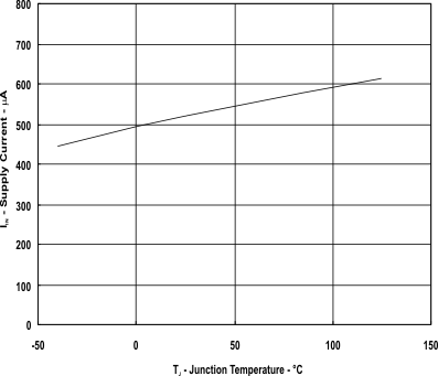
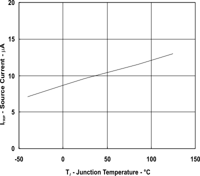
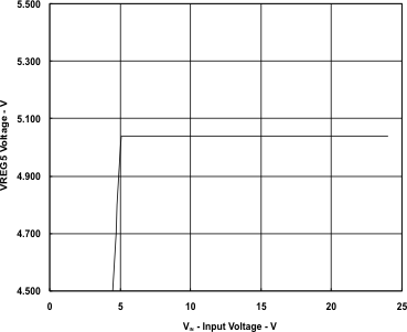
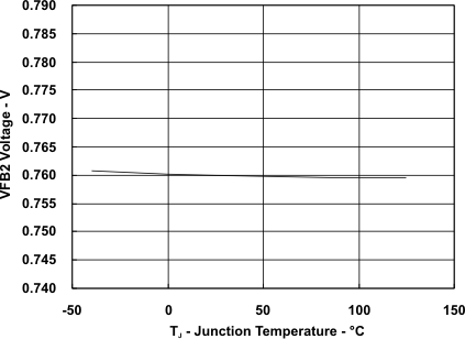
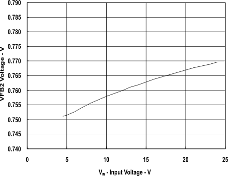
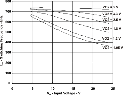
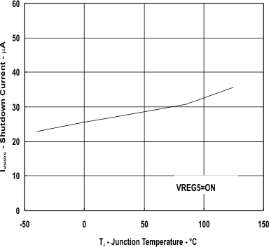
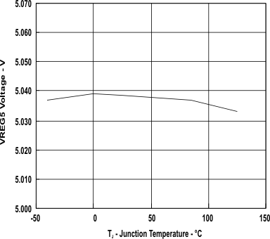
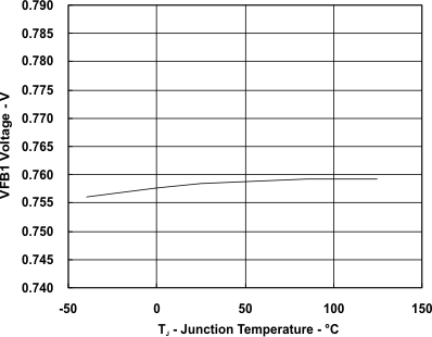
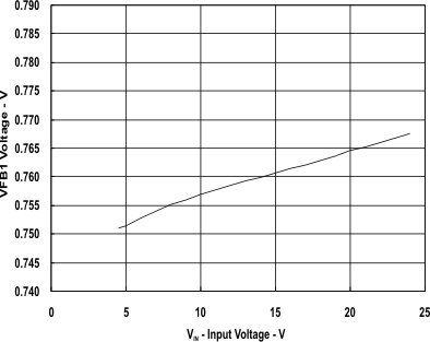
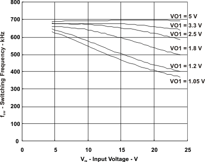
7.8 Typical Characteristics