SLVSBB7E May 2012 – November 2015 TPS54061
PRODUCTION DATA.
- 1 Features
- 2 Applications
- 3 Description
- 4 Revision History
- 5 Pin Configuration and Functions
- 6 Specifications
-
7 Detailed Description
- 7.1 Overview
- 7.2 Functional Block Diagram
- 7.3
Feature Description
- 7.3.1 Fixed Frequency PWM Control
- 7.3.2 Slope Compensation Output Current
- 7.3.3 Error Amplifier
- 7.3.4 Voltage Reference
- 7.3.5 Adjusting the Output Voltage
- 7.3.6 Enable and Adjusting UVLO
- 7.3.7 Internal Slow-Start
- 7.3.8 Constant Switching Frequency and Timing Resistor (RT/CLK Pin)
- 7.3.9 Selecting the Switching Frequency
- 7.3.10 Synchronization to RT/CLK Pin
- 7.3.11 Overvoltage Protection
- 7.3.12 Thermal Shutdown
- 7.4 Device Functional Modes
- 8 Application and Implementation
- 9 Power Supply Recommendations
- 10Layout
- 11Device and Documentation Support
- 12Mechanical, Packaging, and Orderable Information
Package Options
Mechanical Data (Package|Pins)
- DRB|8
Thermal pad, mechanical data (Package|Pins)
- DRB|8
Orderable Information
7 Detailed Description
7.1 Overview
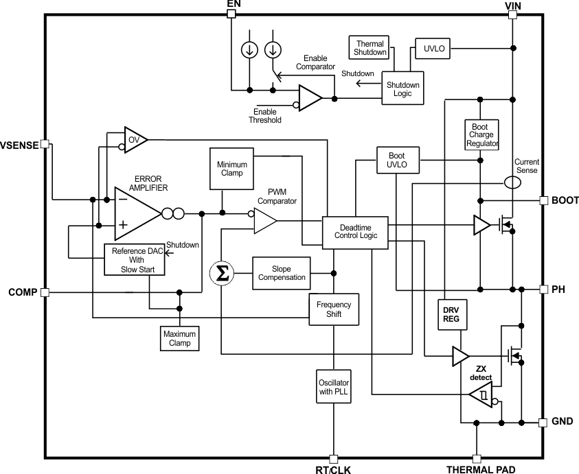
The TPS54061 device is a 60-V, 200-mA, step-down (buck) regulator with an integrated high-side and low-side n-channel MOSFET. To improve performance during line and load transients the device implements a constant frequency, current mode control which reduces output capacitance and simplifies external frequency compensation design.
The switching frequency of 50 kHz to 1100 kHz allows for efficiency and size optimization when selecting the output filter components. The switching frequency is adjusted using a resistor-to-ground on the RT/CLK pin. The device has an internal phase-lock loop (PLL) on the RT/CLK pin that is used to synchronize the power switch turn on to a falling edge of an external system clock.
The TPS54061 has a default startup voltage of approximately 4.5 V. The EN pin has an internal pullup current source that can be used to adjust the input voltage UVLO threshold with two external resistors. In addition, the pullup current provides a default condition. When the EN pin is floating the device will operate. The operating current is 90 µA when not switching and under no load. When the device is disabled, the supply current is 1.4 µA.
The integrated 1.5-Ω high-side MOSFET and 0.8-Ω low-side MOSFET allows for high-efficiency power supply designs capable of delivering 200 milliamperes of continuous current to a load.
The TPS54061 reduces the external component count by integrating the boot recharge diode. The bias voltage for the integrated high-side MOSFET is supplied by a capacitor on the BOOT to PH pin. The boot capacitor voltage is monitored by an UVLO circuit and will turn the high-side MOSFET off when the boot voltage falls below a preset threshold. The TPS54061 can operate at high duty cycles because of the boot UVLO. The output voltage can be adjusted down to as low as the 0.8-V reference.
The TPS54061 has an internal output OV protection that disables the high-side MOSFET if the output voltage is 109% of the nominal output voltage.
The TPS54061 reduces external component count by integrating the slow-start time using a reference DAC system.
The TPS54061 resets the slow-start times during overload conditions with an overload recovery circuit. The overload recovery circuit will slow start the output from the fault voltage to the nominal regulation voltage once a fault condition is removed. A frequency foldback circuit reduces the switching frequency during startup and overcurrent fault conditions to help control the inductor current.
7.2 Functional Block Diagram

7.3 Feature Description
7.3.1 Fixed Frequency PWM Control
The TPS54061 uses adjustable fixed-frequency, peak-current mode control. The output voltage is sensed through external resistors on the VSENSE pin and compared to an internal voltage reference by an error amplifier which drives the COMP pin. An internal oscillator initiates the turn on of the high-side power switch. The error amplifier output is compared to the high-side power switch current. When the power switch current reaches the level set by the COMP voltage, the power switch is turned off. The COMP pin voltage will increase and decrease as the output current increases and decreases. The device implements current limiting by clamping the COMP pin voltage to a maximum level.
7.3.2 Slope Compensation Output Current
The TPS54061 adds a compensating ramp to the switch current signal. This slope compensation prevents sub-harmonic oscillations.
7.3.3 Error Amplifier
The TPS54061 uses a transconductance amplifier for the error amplifier. The error amplifier compares the VSENSE voltage to the lower of the internal slow-start voltage or the internal 0.8-V voltage reference. The transconductance (gm) of the error amplifier is 108 µA/V during normal operation. During the slow-start operation, the transconductance is a fraction of the normal operating gm. The frequency compensation components (capacitor, series resistor and capacitor) are added to the COMP pin-to-ground.
7.3.4 Voltage Reference
The voltage reference system produces a precise voltage reference over temperature by scaling the output of a temperature stable band-gap circuit
7.3.5 Adjusting the Output Voltage
The output voltage is set with a resistor divider from the output node to the VSENSE pin. TI recommends using 1% tolerance or better divider resistors. Start with a 10-kΩ for the RLS resistor and use the Equation 1 to calculate RHS.

7.3.6 Enable and Adjusting UVLO
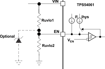
The TPS54061 is enabled when the VIN pin voltage rises above 4.5 V and the EN pin voltage exceeds the EN rising threshold of 1.23 V. The EN pin has an internal pullup current source, I1, of 1.2 µA that provides the default enabled condition when the EN pin floats.
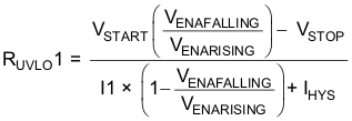
If an application requires a higher input UVLO threshold, use the circuit shown in Figure 18 to adjust the input voltage UVLO with two external resistors. When the EN pin voltage exceeds 1.23 V, an additional 3.5 µA of hysteresis current, Ihys, is sourced out of the EN pin. When the EN pin is pulled below 1.18 V, the 3.5-µA Ihys current is removed. This additional current facilitates adjustable input voltage hysteresis. Use Equation 2 to calculate RUVLO1 for the desired input start and stop voltages . Use Equation 3 to similarly calculate RUVLO2.
In applications designed to start at relatively low input voltages (for example, from 4.7 V to 10 V) and withstand high input voltages (for example, from 40 V to 60 V), the EN pin may experience a voltage greater than the absolute maximum voltage of 8 V during the high input voltage condition. TI recommends using a zener diode to clamp the pin voltage below the absolute maximum rating.
 Figure 18. Adjustable Undervoltage Lock-Out


7.3.7 Internal Slow-Start
The TPS54061 has an internal digital slow-start that ramps the reference voltage from zero volts to its final value in 1114 switching cycles. The internal slow-start time is calculated by the following expression:

If the EN pin is pulled below the stop threshold of 1.18 V, switching stops and the internal slow-start resets. The slow-start also resets in thermal shutdown.
7.3.8 Constant Switching Frequency and Timing Resistor (RT/CLK Pin)
The switching frequency of the TPS54061 is adjustable over a wide range from 50 kHz to 1100 kHz by varying the resistor on the RT/CLK pin. The RT/CLK pin voltage is typically 0.53 V and must have a resistor-to-ground to set the switching frequency. To determine the timing resistance for a given switching frequency, use Equation 5. To reduce the solution size, one would typically set the switching frequency as high as possible, but tradeoffs of the supply efficiency, maximum input voltage and minimum controllable on-time should be considered. The minimum controllable on-time is typically 120 ns and limits the operating frequency for high input voltages. The maximum switching frequency is also limited by the frequency shift circuit. More discussion on the details of the maximum switching frequency is located below.

7.3.9 Selecting the Switching Frequency
The TPS54061 implements current-mode control which uses the COMP pin voltage to turn off the high-side MOSFET on a cycle-by-cycle basis. Each cycle the switch current and COMP pin voltage are compared, when the peak switch current intersects the COMP voltage, the high-side switch is turned off. During overcurrent conditions that pull the output voltage low, the error amplifier will respond by driving the COMP pin high, increasing the switch current. The error amplifier output is clamped internally, which functions as a switch current limit.
To enable higher switching frequency at high input voltages, the TPS54061 implements a frequency shift. The switching frequency is divided by 8, 4, 2, and 1 as the voltage ramps from 0 to 0.8 volts on VSENSE pin. The device implements a digital frequency shift to enable synchronizing to an external clock during normal startup and fault conditions. Because the device can only divide the switching frequency by 8, there is a maximum input voltage limit in which the device operates and still have frequency shift protection. During short-circuit events (particularly with high input voltage applications), the control loop has a finite minimum controllable on-time and the output has a low voltage. During the switch-on time, the inductor current ramps to the peak current limit because of the high input voltage and minimum on-time. During the switch-off time, the inductor would normally not have enough off-time and output voltage for the inductor to ramp down by the ramp up amount. The frequency shift effectively increases the off-time allowing the current to ramp down.


where
- IO = Output current
- ICL = Current Limit
- VIN = Input Voltage
- VOUT = Output Voltage
- VOUTSC Output Voltage during short
- RDC = Inductor resistance
- RHS = High-side MOSFET resistance
- RLS = Low-side MOSFET resistance
- ton = Controllable on-time
- fdiv = Frequency divide (equals 1, 2, 4, or 8)
7.3.10 Synchronization to RT/CLK Pin
The RT/CLK pin can be used to synchronize the regulator to an external system clock. To implement the synchronization feature connect a square wave to the RT/CLK pin through one of the circuit networks shown in Figure 19. The square-wave amplitude must extend lower than 0.5 V and higher than 1.8 V on the RT/CLK pin and have high and low states greater than 40 ns. The synchronization frequency range is 300 kHz to 1100 kHz. The rising edge of the PH will be synchronized to the falling edge of RT/CLK pin signal. The external synchronization circuit should be designed in such a way that the device will have the default frequency set resistor connected from the RT/CLK pin-to-ground should the synchronization signal turn off. TI recommends using a frequency set resistor connected as shown in Figure 19 through another resistor-to-ground (e.g., 50 Ω) for clock signal that are not Hi-Z or tristate during the off state. The sum of the resistance should set the switching frequency close to the external CLK frequency. TI recommends to AC couple the synchronization signal through a 10-pF ceramic capacitor to RT/CLK pin. The first time the CLK is pulled above the CLK threshold the device switches from the RT resistor frequency to PLL mode. The internal 0.5 V voltage source is removed and the CLK pin becomes high impedance as the PLL starts to lock onto the external signal. The switching frequency can be higher or lower than the frequency set with the RT/CLK resistor. The device transitions from the resistor mode to the PLL mode and lock onto the CLK frequency within 100 microseconds. When the device transitions from the PLL mode to the resistor mode, the switching frequency will reduce from the external CLK frequency to 150 kHz, then reapply the 0.5-V voltage source and the resistor will then set the switching frequency. The switching frequency is divided by 8, 4, 2, and 1 as the voltage ramps from 0 to 0.8 volts on VSENSE pin. The device implements a digital frequency shift to enable synchronizing to an external clock during normal startup and fault conditions.
 Figure 19. Synchronizing to a System Clock
7.3.11 Overvoltage Protection
The TPS54061 incorporates an output overvoltage transient protection (OVP) circuit to minimize voltage overshoot when recovering from output fault conditions or strong unload transients on power supply designs with low-value output capacitance. For example, when the power supply output is overloaded the error amplifier compares the actual output voltage to the internal reference voltage. If the VSENSE pin voltage is lower than the internal reference voltage for a considerable time, the output of the error amplifier will respond by clamping the error amplifier output to a high voltage. Thus, requesting the maximum output current. Once the condition is removed, the regulator output rises and the error amplifier output transitions to the steady-state duty cycle. In some applications, the power supply output voltage can respond faster than the error amplifier output can respond, this actuality leads to the possibility of an output overshoot.
The OVP feature minimizes the output overshoot when using a low-value output capacitor by comparing the VSENSE pin voltage to OVP threshold which is 109% of the internal voltage reference. If the VSENSE pin voltage is greater than the OVP threshold, the high-side MOSFET is disabled to minimize output overshoot. When the VSENSE voltage drops lower than the OVP threshold, the high-side MOSFET resumes normal operation.
7.3.12 Thermal Shutdown
The device implements an internal thermal shutdown until the junction temperature exceeds 176°C. The thermal shutdown forces the device to stop switching until the junction temperature falls below the thermal trip threshold. Once the die temperature decreases below 176°C, the device reinitiates the power-up sequence by restarting the internal slow-start.
7.4 Device Functional Modes
7.4.1 Operation Near Minimimum Input Voltage
The TPS54061 is recommended to operate with input voltages above 4.7 V. The typical VIN UVLO threshold is 4.5 V and the device may operate at input voltages down to the UVLO voltage. At input voltages below the actual UVLO voltage the device will not switch. If EN is floating or externally pulled up to greater up than the typical 1.23 V rising threshold, when V(VIN) passes the UVLO threshold the TPS54061 will become active. Switching is enabled and the slow-start sequence is initiated. The TPS54061 starts linearly ramping up the internal reference DAC from 0 V to the reference voltage over the internal slow-start time period set by the switching frequency.
7.4.2 Operation With Enable Control
The enable start threshold voltage is 1.23 V typical. With EN held below the 1.23 V typical rising threshold voltage the TPS54061 is disabled and switching is inhibited even if VIN is above its UVLO threshold. The quiescent current is reduced in this state. If the EN voltage is increased above the rising threshold voltage while V(VIN) is above the UVLO threshold, the device becomes active. Switching is enabled and the slow-start sequence is initiated. The TPS54061 starts linearly ramping up the internal reference DAC from 0 V to the reference voltage over the internal slow-start time period set by the switching frequency. If EN is pulled below the 1.18 V typical falling threshold the TPS54061 will enter the reduced quiescent current state again.