SLVSBB7E May   2012  – November 2015 TPS54061

PRODUCTION DATA.  

  1. Features
  2. Applications
  3. Description
  4. Revision History
  5. Pin Configuration and Functions
  6. Specifications
    1. 6.1 Absolute Maximum Ratings
    2. 6.2 ESD Ratings
    3. 6.3 Recommended Operating Conditions
    4. 6.4 Thermal Information
    5. 6.5 Electrical Characteristics
    6. 6.6 Typical Characteristics
  7. Detailed Description
    1. 7.1 Overview
    2. 7.2 Functional Block Diagram
    3. 7.3 Feature Description
      1. 7.3.1  Fixed Frequency PWM Control
      2. 7.3.2  Slope Compensation Output Current
      3. 7.3.3  Error Amplifier
      4. 7.3.4  Voltage Reference
      5. 7.3.5  Adjusting the Output Voltage
      6. 7.3.6  Enable and Adjusting UVLO
      7. 7.3.7  Internal Slow-Start
      8. 7.3.8  Constant Switching Frequency and Timing Resistor (RT/CLK Pin)
      9. 7.3.9  Selecting the Switching Frequency
      10. 7.3.10 Synchronization to RT/CLK Pin
      11. 7.3.11 Overvoltage Protection
      12. 7.3.12 Thermal Shutdown
    4. 7.4 Device Functional Modes
      1. 7.4.1 Operation Near Minimimum Input Voltage
      2. 7.4.2 Operation With Enable Control
  8. Application and Implementation
    1. 8.1 Application Information
    2. 8.2 Typical Applications
      1. 8.2.1 CCM Application
        1. 8.2.1.1 Design Requirements
        2. 8.2.1.2 Detailed Design Procedure
          1. 8.2.1.2.1 Selecting the Switching Frequency
          2. 8.2.1.2.2 Output Inductor Selection (LO)
          3. 8.2.1.2.3 Output Capacitor
          4. 8.2.1.2.4 Input Capacitor
          5. 8.2.1.2.5 Bootstrap Capacitor Selection
          6. 8.2.1.2.6 UVLO Set Point
          7. 8.2.1.2.7 Output Voltage and Feedback Resistors Selection
          8. 8.2.1.2.8 Closing the Loop
        3. 8.2.1.3 Application Curves
      2. 8.2.2 DCM Application
        1. 8.2.2.1 Design Requirements
        2. 8.2.2.2 Detailed Design Procedure
          1. 8.2.2.2.1 Designing an Efficient, Low-Output Current Power Supply at a Fixed Switching Frequency
          2. 8.2.2.2.2 Closing the Feedback Loop
        3. 8.2.2.3 Application Curves
  9. Power Supply Recommendations
  10. 10Layout
    1. 10.1 Layout Guidelines
    2. 10.2 Layout Example
  11. 11Device and Documentation Support
    1. 11.1 Trademarks
    2. 11.2 Electrostatic Discharge Caution
    3. 11.3 Glossary
  12. 12Mechanical, Packaging, and Orderable Information

Package Options

Mechanical Data (Package|Pins)
Thermal pad, mechanical data (Package|Pins)
Orderable Information

6 Specifications

6.1 Absolute Maximum Ratings

over operating free-air temperature (unless otherwise noted)(1)
MIN MAX UNIT
Voltage VIN –0.3 62 V
EN(2) –0.3 8 V
BOOT-PH –0.3 8 V
VSENSE –0.3 6 V
COMP –0.3 3 V
PH –0.6 62 V
PH, 10ns Transient –4 62 V
RT/CLK –0.3 6 V
Current VIN Internally Limited A
BOOT 100 mA
PH Internally Limited A
Operating junction temperature –40 150 ºC
Storage temperature, Tstg –65 150 °C
(1) Stresses beyond those listed under Absolute Maximum Ratings may cause permanent damage to the device. These are stress ratings only, which do not imply functional operation of the device at these or any other conditions beyond those indicated under Recommended Operating Conditions. Exposure to absolute-maximum-rated conditions for extended periods may affect device reliability.

6.2 ESD Ratings

VALUE UNIT
V(ESD) Electrostatic discharge Human body model (HBM), per ANSI/ESDA/JEDEC JS-001, all pins(1) ±2000 V
Charged device model (CDM), per JEDEC specification JESD22-C101, all pins(2) ±500
(1) JEDEC document JEP155 states that 500-V HBM allows safe manufacturing with a standard ESD control process.
(2) JEDEC document JEP157 states that 250-V CDM allows safe manufacturing with a standard ESD control process.

6.3 Recommended Operating Conditions

over operating free-air temperature range (unless otherwise noted)
MIN MAX UNIT
Input coltage 4.7 60 V
Output current 200 mA
Switching frequency set by RT/CLK resistor 50 1100 kHz
Switching frequency synchronized to external clock 300 1100 kHz

6.4 Thermal Information

THERMAL METRIC(1) TPS54061 UNIT
DRB
8 PINS
RθJA Junction-to-ambient thermal resistance 42.9 °C/W
RθJC(top) Junction-to-case (top) thermal resistance 46.0
RθJB Junction-to-board thermal resistance 18.1
ψJT Junction-to-top characterization parameter 0.5
ψJB Junction-to-board characterization parameter 18.3
RθJC(bot) Junction-to-case (bottom) thermal resistance 3.0
(1) For more information about traditional and new thermal metrics, see the IC Package Thermal Metrics application report, SPRA953.

6.5 Electrical Characteristics(1)

TJ = –40°C to 150°C, VIN = 4.7 to 60 V (unless otherwise noted)
PARAMETER TEST CONDITIONS MIN TYP MAX UNIT
SUPPLY VOLTAGE (VIN PIN)
Operating input voltage VIN 4.7 60 V
Shutdown supply current EN = 0 V 1.4 µA
Iq Operating – Non switching VSENSE = 0.9 V, VIN = 12 V 90 110 µA
ENABLE AND UVLO (EN PIN)
Enable threshold Rising 1.23 1.4 V
Falling 1 1.18 V
Input current Enable threshold +50 mV –4.7 µA
Enable threshold –50 mV –1.2 µA
Hysteresis –3.5 µA
Enable high to start switching time 450 µs
VIN
VIN start voltage VIN rising 4.5 V
VOLTAGE REFERENCE
Voltage reference TJ = 25°C, VIN = 12 V 0.792 0.8 0.808 V
1mA < IOUT < Minimum Current Limit 0.784 0.8 0.816
HIGH-SIDE MOSFET
Switch resistance BOOT-PH = 5.7 V 1.5 3.0 Ω
LOW-SIDE MOSFET
Switch resistance VIN = 12 V 0.8 1.5 Ω
ERROR AMPLIFIER
Input Current VSENSE pin 20 nA
Error amp gm –2µA < I(COMP) < 2µA, V(COMP) = 1 V 108 µS
EA gm during slow start –2 µA < I(COMP) < 2 µA, V(COMP) = 1 V, VSENSE = 0.4 V 27 µS
Error amp DC gain VSENSE = 0.8V 1000 V/V
Min unity gain bandwidth 0.5 MHz
Error amp source/sink V(COMP) = 1 V, 100 mV Overdrive ±8 µA
Start-Switching Threshold 0.57 V
COMP to Iswitch gm 1.0 A/V
CURRENT LIMIT
High-side sourcing current limit threshold BOOT-PH = 5.7 V 250 350 500 mA
Zero cross detect current –1.1 mA
THERMAL SHUTDOWN
Thermal shutdown 176 C
RT/CLK
Operating frequency using RT mode 50 1100 kHz
Switching frequency R(RT/CLK) = 120 kΩ 425 472 520 kHz
Minimum CLK pulsewidth 40 ns
RT/CLK voltage R(RT/CLK) = 120 kΩ 0.53 V
RT/CLK high threshold 1.8 V
RT/CLK low threshold 0.5 V
RT/CLK falling edge to PH rising edge delay Measure at 500 kHz with RT resistor 60 ns
PLL lock in time Measure at 500 kHz 100 µs
PLL frequency range 300 1100 kHz
PH
Minimum On-time Measured at 50% to 50%, IOUT = 200 mA 120 ns
Dead time VIN = 12 V, IOUT = 200 mA, One transition 30 ns
BOOT
BOOT to PH regulation voltage VIN = 12 V 6.0 V
BOOT-PH UVLO 2.9 V
INTERNAL SLOW-START TIME
Slow-Start time fSW = 472 kHz, RT = 120 kΩ, 10% to 90% 2.36 ms
(1) The Electrical Characteristics specified in this section will apply to all specifications in this document unless otherwise noted.

6.6 Typical Characteristics
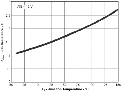
TPS54061 res_tj_lvsbb7.gif
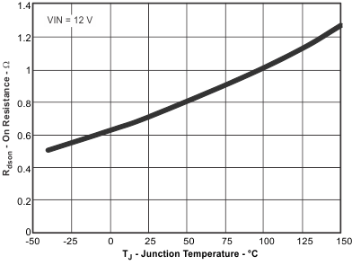
Figure 1. High-Side RDS(on) vs Temperature
TPS54061 vref_tj_lvsbb7.gif
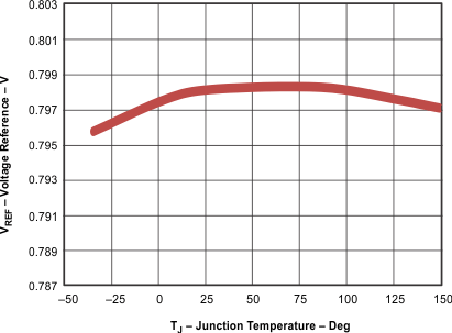
Figure 3. VREF Voltage vs Temperature
TPS54061 fsw_tj_lvsbb7.gif
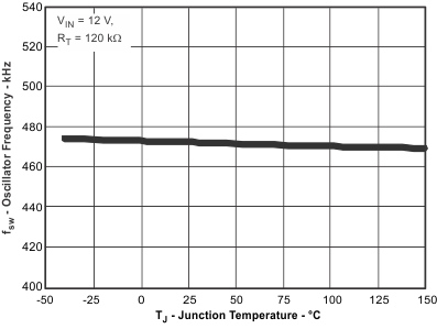
Figure 5. Frequency vs Temperature
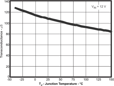
TPS54061 trns_tj_lvsbb7.gif
Figure 7. Error Amp Transconductance vs Temperature
TPS54061 hys_curr_tj_lvsbb7.gif
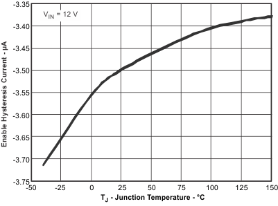
Figure 9. Enable Pin Hysteresis Current
vs Temperature
TPS54061 curr_vi_lvsbb7.gif
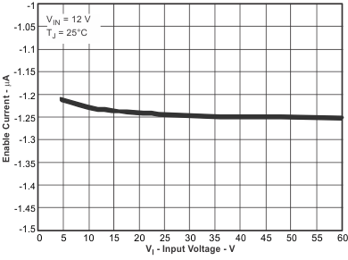
Figure 11. Enable Pin Pullup Current vs Input Voltage
TPS54061 G003_SLVSBB7.png
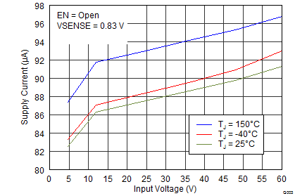
Figure 13. Supply Current (VIN Pin) vs Input Voltage
TPS54061 icc3_vi_lvsbb7.gif
A.
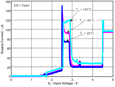
Figure 15. Supply Current (VIN Pin) vs
Input Voltage (0 V to VSTART) En Pin Open
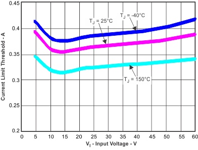
TPS54061 curr2_vi_lvsbb7.gif
Figure 17. Current Limit vs Input Voltage
TPS54061 res_LS_tj_lvsbb7.gif
Figure 2. Low-Side RDS(on) vs Temperature
TPS54061 fsw_v_lvsbb7.gif
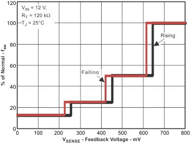
Figure 4. Frequency vs Vsense Voltage
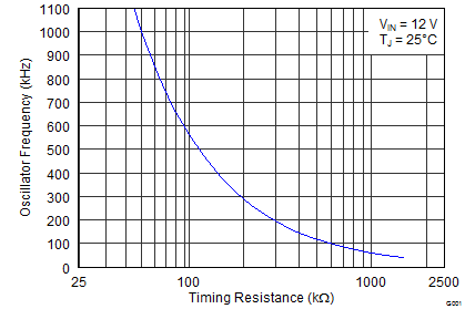
TPS54061 G001_SLVSBB7.png
Figure 6. Frequency vs RT/CLK Resistance
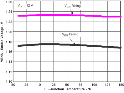
TPS54061 VENA_tj_lvsbb7.gif
Figure 8. Enable Pin Voltage vs Temperature
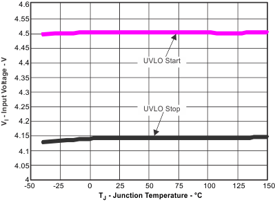
TPS54061 vi_tj_lvsbb7.gif
Figure 10. Input Voltage (UVLO) vs Temperature
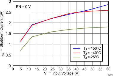
TPS54061 Isd_shutdn_vin_lvsbb7.gif
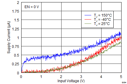
Figure 12. Shutdown Supply Current (VIN) vs Input Voltage
TPS54061 G004_SLVSBB7.png
A.
Figure 14. Supply Current (VIN Pin)
vs Input Voltage (0 V to VSTART) En Pin Low
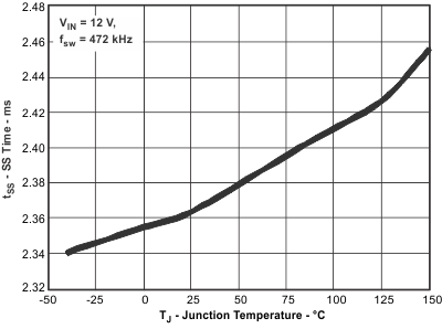
TPS54061 ss_tj_lvsbb7.gif
Figure 16. Slow-Start Time vs Temperature