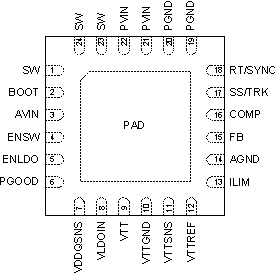
| SW |
1, 23, 24 |
O |
Switching node of the buck converter. |
| BOOT |
2 |
I |
Bootstrap capacitor node for high-side MOSFET gate driver of the buck converter. Connect the bootstrap capacitor from this pin to the SW pin. |
| AVIN |
3 |
I |
The input supply pin to the IC, powering the control circuits of both the buck converter and DDR termination regulator. Connect AVIN to a supply voltage between 2.95 V and 6 V. |
| ENSW |
4 |
I |
Buck converter enable pin with internal pull-up current source. Floating this pin will enable the IC. Pull below 1.17 V to enter low current standby mode. Pull below 0.4 V to enter shutdown mode. The ENSW pin can be used to implement adjustable under-voltage lockout (UVLO) using two resistors. |
| ENLDO |
5 |
I |
VTT LDO enable pin with internal pull-up current source. Floating this pin will enable the IC. Pull below 1.17 V to enter low current standby mode. Pull below 0.4 V to enter shutdown mode. The ENLDO pin can be used to implement adjustable under-voltage lockout (UVLO) using two resistors. |
| PGOOD |
6 |
O |
Power good indicator for the buck regulator. This pin is an open-drain output. A 10-kΩ pull-up resistor is recommended between PGOOD and AVIN or an external logic supply pin. |
| VDDQSNS |
7 |
I |
VDDQ sense input to generate VDDQ/2 reference for VTTREF. |
| LDOIN |
8 |
I |
Power supply input for VTT LDO. Connected VDDQ in typical application. Alternatively this pin can be used for split-rail configuration to reduce power dissipation when sourcing current to the VTT output by powering the VTT LDO with a lower voltage. |
| VTT |
9 |
O |
1-A LDO output. Connect 2 x 10-µF ceramic capacitors to VTTGND for stability. |
| VTTGND |
10 |
I |
Power ground for VTT LDO. |
| VTTSNS |
11 |
I |
VTT LDO voltage feedback. |
| VTTREF |
12 |
O |
Buffered low-noise VTT reference output. Connect to a 0.22 µF or larger ceramic capacitor to AGND for stability. |
| ILIM |
13 |
I |
Programmable current limit pin. An internal amplifier holds this pin at a fixed voltage then sets the high-side MOSFET peak current limit based on the value of an external resistor to AGND. |
| AGND |
14 |
I |
Analog signal ground of the IC. AGND should be connected to PGND via a single point on the PCB, typically to the thermal pad. |
| FB |
15 |
I |
Error amplifier inverting input and feedback pin for voltage regulation of the buck converter. Connect this pin to the center of a resistor divider to set the output voltage of the buck converter. The resistor divider should go from the regulated output voltage to AGND. |
| COMP |
16 |
I |
Output of the internal transconductance error amplifier for the buck converter. The feedback loop compensation network is connected from this pin to AGND. |
| SS/TRK |
17 |
I |
Soft-start programming pin. A capacitor between the SS/TRK pin and AGND pin sets soft-start time. The voltage on this pin overrides the internal reference allowing it to be used for tracking and sequencing. |
| RT/SYNC |
18 |
I |
Resistor Timing and External Clock. An internal amplifier holds this pin at a fixed voltage when using an external resistor to AGND to set the switching frequency. If the pin is pulled above the upper threshold, a mode change occurs and the pin becomes a synchronization input. The internal amplifier is disabled and the pin is a high impedance clock input. If clocking edges stop, the internal amplifier is re-enabled and the operating mode returns to resistor frequency programming. |
| PGND |
19, 20 |
I |
Power ground of the buck regulator. PGND should be connected to AGND via a single point on PCB board, typically to the thermal pad. |
| PVIN |
21, 22 |
I |
The input supply pin for power MOSFETs. Connect PVIN to a supply voltage between 2.95 V and 6 V. |
| PAD |
– |
The exposed thermal pad must be electrically connected to AGND and PGND on the printed circuit board for proper operation. Connect to the largest possible copper area for best thermal performance. |
