SLVSAA6B April 2010 – November 2014 TPS54240
PRODUCTION DATA.
- 1 Features
- 2 Applications
- 3 Description
- 4 Revision History
- 5 Pin Configuration and Functions
- 6 Specifications
-
7 Detailed Description
- 7.1 Overview
- 7.2 Functional Block Diagram
- 7.3
Feature Description
- 7.3.1 Fixed Frequency PWM Control
- 7.3.2 Slope Compensation Output Current
- 7.3.3 Pulse Skip Eco-Mode
- 7.3.4 Low Dropout Operation and Bootstrap Voltage (BOOT)
- 7.3.5 Error Amplifier
- 7.3.6 Voltage Reference
- 7.3.7 Adjusting The Output Voltage
- 7.3.8 Enable And Adjusting Undervoltage Lockout
- 7.3.9 Slow-Start / Tracking Pin (SS/TR)
- 7.3.10 Overload Recovery Circuit
- 7.3.11 Sequencing
- 7.3.12 Constant Switching Frequency and Timing Resistor (RT/CLK Pin)
- 7.3.13 Overcurrent Protection and Frequency Shift
- 7.3.14 Selecting the Switching Frequency
- 7.3.15 How to Interface to RT/CLK Pin
- 7.3.16 Powergood (PWRGD Pin)
- 7.3.17 Overvoltage Transient Protection
- 7.3.18 Thermal Shutdown
- 7.3.19 Small Signal Model for Loop Response
- 7.3.20 Simple Small Signal Model for Peak Current Mode Control
- 7.3.21 Small Signal Model for Frequency Compensation
- 7.4 Device Functional Modes
-
8 Application and Implementation
- 8.1 Application Information
- 8.2
Typical Application
- 8.2.1
TPS54240 3.3-V Output Design
- 8.2.1.1 Design Requirements
- 8.2.1.2
Detailed Design Procedure
- 8.2.1.2.1 Selecting the Switching Frequency
- 8.2.1.2.2 Output Inductor Selection (LO)
- 8.2.1.2.3 Output Capacitor
- 8.2.1.2.4 Catch Diode
- 8.2.1.2.5 Input Capacitor
- 8.2.1.2.6 Slow-Start Capacitor
- 8.2.1.2.7 Bootstrap Capacitor Selection
- 8.2.1.2.8 Undervoltage Lock Out Set Point
- 8.2.1.2.9 Output Voltage And Feedback Resistors Selection
- 8.2.1.2.10 Compensation
- 8.2.1.2.11 Discontinuous Mode And Eco-Mode Boundary
- 8.2.1.2.12 Power Dissipation Estimate
- 8.2.1.3 Application Curves
- 8.2.2 TPS54240 Inverting Power Supply
- 8.2.3 TPS54240 Split Rail Power Supply
- 8.2.4 12-V To 3.8-V GSM Power Supply
- 8.2.5 24-V to 4.2-V GSM Power Supply
- 8.2.1
TPS54240 3.3-V Output Design
- 9 Power Supply Recommendations
- 10Layout
- 11Device and Documentation Support
- 12Mechanical, Packaging, and Orderable Information
Package Options
Mechanical Data (Package|Pins)
Thermal pad, mechanical data (Package|Pins)
Orderable Information
8 Application and Implementation
NOTE
Information in the following applications sections is not part of the TI component specification, and TI does not warrant its accuracy or completeness. TI’s customers are responsible for determining suitability of components for their purposes. Customers should validate and test their design implementation to confirm system functionality.
8.1 Application Information
The TPS54240 device is a 42-V, 2.5-A, step-down regulator with an integrated high-side MOSFET. This device typically converts a higher DC voltage to a lower DC voltage with a maximum available output current of 2.5 A. Example applications are 12-V and 24-V industrial, automotive and communication power systems. Use the following design procedure to select component values for the TPS54240 device. This procedure illustrates the design of a high-frequency switching regulator using ceramic output capacitors. The Excel™ spreadsheet (SLVC432) located on the product page can help on all calculations. Alternatively, use the WEBENCH software to generate a complete design. The WEBENCH software uses an iterative design procedure and accesses a comprehensive database of components when generating a design.
8.2 Typical Application
8.2.1 TPS54240 3.3-V Output Design
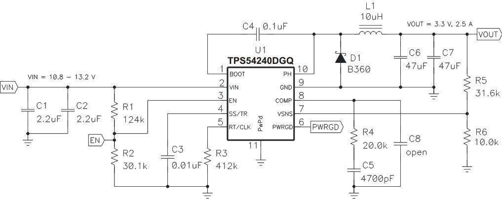 Figure 49. 3.3-V Output TPS54240 Design Example
8.2.1.1 Design Requirements
This example details the design of a high-frequency switching regulator design using ceramic output capacitors. A few parameters must be known in order to start the design process. These parameters are typically determined at the system level. For this example, we will start with the following known parameters:
8.2.1.2 Detailed Design Procedure
8.2.1.2.1 Selecting the Switching Frequency
The first step is to decide on a switching frequency for the regulator. Typically, the user will want to choose the highest switching frequency possible since this will produce the smallest solution size. The high-switching frequency allows for lower valued inductors and smaller output capacitors compared to a power supply that switches at a lower frequency. The switching frequency that can be selected is limited by the minimum on-time of the internal power switch, the input voltage and the output voltage and the frequency shift limitation.
Equation 12 and Equation 13 must be used to find the maximum switching frequency for the regulator, choose the lower value of the two equations. Switching frequencies higher than these values will result in pulse skipping or the lack of overcurrent protection during a short circuit.
The typical minimum on time, tonmin, is 135 ns for the TPS54240. For this example, the output voltage is 3.3 V and the maximum input voltage is 13.2 V, which allows for a maximum switch frequency up to 2247 kHz when including the inductor resistance, on resistance output current and diode voltage in Equation 12. To ensure overcurrent runaway is not a concern during short circuits in your design use Equation 13 or the solid curve in Figure 40 to determine the maximum switching frequency. With a maximum input voltage of 13.2 V, assuming a diode voltage of 0.7 V, inductor resistance of 26 mΩ, switch resistance of 200 mΩ, a current limit value of 3.5 A and a short circuit output voltage of 0.2 V. The maximum switching frequency is approximately 4449 kHz.
For this design, a much lower switching frequency of 300 kHz is used. To determine the timing resistance for a given switching frequency, use Equation 11 or the curve in Figure 39.
The switching frequency is set by resistor R3 shown in Figure 49 For 300-kHz operation a 412-kΩ resistor is required.
8.2.1.2.2 Output Inductor Selection (LO)
To calculate the minimum value of the output inductor, use Equation 28.
KIND is a coefficient that represents the amount of inductor ripple current relative to the maximum output current.
The inductor ripple current will be filtered by the output capacitor. Therefore, choosing high-inductor ripple currents will impact the selection of the output capacitor since the output capacitor must have a ripple current rating equal to or greater than the inductor ripple current. In general, the inductor ripple value is at the discretion of the designer; however, the following guidelines may be used.
For designs using low ESR output capacitors such as ceramics, a value as high as KIND = 0.3 may be used. When using higher ESR output capacitors, KIND = 0.2 yields better results. Since the inductor ripple current is part of the PWM control system, the inductor ripple current should always be greater than 150 mA for dependable operation. In a wide-input voltage regulator, it is best to choose an inductor ripple current on the larger side. This allows the inductor to still have a measurable ripple current with the input voltage at its minimum.
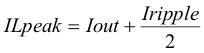
For this design example, use KIND = 0.3 and the minimum inductor value is calculated to be 11 μH. For this design, a nearest standard value was chosen: 10 μH. For the output filter inductor, it is important that the RMS current and saturation current ratings not be exceeded. The RMS and peak inductor current can be found from Equation 30 and Equation 31.
For this design, the RMS inductor current is 2.51 A and the peak inductor current is 2.913 A. The chosen inductor is a Coilcraft MSS1038-103NLB . It has a saturation current rating of 4.52 A and an RMS current rating of 4.05 A.
As the equation set demonstrates, lower ripple currents will reduce the output voltage ripple of the regulator but will require a larger value of inductance. Selecting higher ripple currents will increase the output voltage ripple of the regulator but allow for a lower inductance value.
The current flowing through the inductor is the inductor ripple current plus the output current. During power-up, faults or transient load conditions, the inductor current can increase above the calculated peak inductor current level calculated above. In transient conditions, the inductor current can increase up to the switch current limit of the device. For this reason, the most conservative approach is to specify an inductor with a saturation current rating equal to or greater than the switch current limit rather than the peak inductor current.
8.2.1.2.3 Output Capacitor
There are three primary considerations for selecting the value of the output capacitor. The output capacitor will determine the modulator pole, the output voltage ripple, and how the regulators responds to a large change in load current. The output capacitance needs to be selected based on the more stringent of these three criteria.
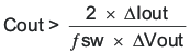
The desired response to a large change in the load current is the first criteria. The output capacitor needs to supply the load with current when the regulator cannot. This situation would occur if there are desired hold-up times for the regulator where the output capacitor must hold the output voltage above a certain level for a specified amount of time after the input power is removed. The regulator also will temporarily not be able to supply sufficient output current if there is a large, fast increase in the current needs of the load such as transitioning from no load to a full load. The regulator usually needs two or more clock cycles for the control loop to see the change in load current and output voltage and adjust the duty cycle to react to the change. The output capacitor must be sized to supply the extra current to the load until the control loop responds to the load change. The output capacitance must be large enough to supply the difference in current for two clock cycles while only allowing a tolerable amount of droop in the output voltage. Equation 32 shows the minimum output capacitance necessary to accomplish this.
Where ΔIout is the change in output current, ƒsw is the regulators switching frequency and ΔVout is the allowable change in the output voltage. For this example, the transient load response is specified as a 3% change in Vout for a load step from 1.5 A to 2.5 A (full load). For this example, ΔIout = 2.5-1.5 = 1.0 A and ΔVout = 0.03 × 3.3 = 0.099 V. Using these numbers gives a minimum capacitance of 67 μF. This value does not take the ESR of the output capacitor into account in the output voltage change. For ceramic capacitors, the ESR is usually small enough to ignore in this calculation. Aluminum electrolytic and tantalum capacitors have higher ESR that should be taken into account.
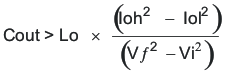
The catch diode of the regulator cannot sink current so any stored energy in the inductor will produce an output voltage overshoot when the load current rapidly decreases, see Figure 50. The output capacitor must also be sized to absorb energy stored in the inductor when transitioning from a high load current to a lower load current. The excess energy that gets stored in the output capacitor will increase the voltage on the capacitor. The capacitor must be sized to maintain the desired output voltage during these transient periods. Equation 33 is used to calculate the minimum capacitance to keep the output voltage overshoot to a desired value. Where L is the value of the inductor, IOH is the output current under heavy load, IOL is the output under light load, Vf is the final peak output voltage, and Vi is the initial capacitor voltage. For this example, the worst case load step will be from 2.5 A to 1.5 A. The output voltage will increase during this load transition and the stated maximum in our specification is 3 % of the output voltage. This will make Vf = 1.03 × 3.3 = 3.399 V. Vi is the initial capacitor voltage which is the nominal output voltage of 3.3 V. Using these numbers in Equation 33 yields a minimum capacitance of 60 μF.
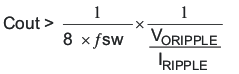
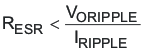
Equation 34 calculates the minimum output capacitance needed to meet the output voltage ripple specification. Where fsw is the switching frequency, Voripple is the maximum allowable output voltage ripple, and Iripple is the inductor ripple current. Equation 34 yields 12 μF.
Equation 35 calculates the maximum ESR an output capacitor can have to meet the output voltage ripple specification. Equation 35 indicates the ESR should be less than 36 mΩ.
The most stringent criteria for the output capacitor is 67 μF of capacitance to keep the output voltage in regulation during an load transient.
Additional capacitance de-ratings for aging, temperature and DC bias should be factored in which will increase this minimum value. For this example, 2 x 47-μF, 10-V ceramic capacitors with 3 mΩ of ESR will be used. The derated capacitance is 72.4 µF, above the minimum required capacitance of 67 µF.
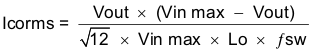
Capacitors generally have limits to the amount of ripple current they can handle without failing or producing excess heat. An output capacitor that can support the inductor ripple current must be specified. Some capacitor data sheets specify the Root Mean Square (RMS) value of the maximum ripple current. Equation 36 can be used to calculate the RMS ripple current the output capacitor needs to support. For this application, Equation 36 yields 238 mA.
8.2.1.2.4 Catch Diode
The TPS54240 requires an external catch diode between the PH pin and GND. The selected diode must have a reverse voltage rating equal to or greater than Vinmax. The peak current rating of the diode must be greater than the maximum inductor current. The diode should also have a low-forward voltage. Schottky diodes are typically a good choice for the catch diode due to their low-forward voltage. The lower the forward voltage of the diode, the higher the efficiency of the regulator.
Typically, the higher the voltage and current ratings the diode has, the higher the forward voltage will be. Although the design example has an input voltage up to 13.2 V, a diode with a minimum of 60-V reverse voltage is selected.
For the example design, the B360B-13-F Schottky diode is selected for its lower-forward voltage and it comes in a larger package size which has good thermal characteristics over small devices. The typical forward voltage of the B360B-13-F is 0.70 volts.
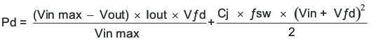
The diode must also be selected with an appropriate power rating. The diode conducts the output current during the off-time of the internal power switch. The off-time of the internal switch is a function of the maximum input voltage, the output voltage, and the switching frequency. The output current during the off-time is multiplied by the forward voltage of the diode which equals the conduction losses of the diode. At higher switch frequencies, the AC losses of the diode need to be taken into account. The AC losses of the diode are due to the charging and discharging of the junction capacitance and reverse recovery. Equation 37 is used to calculate the total power dissipation, conduction losses plus SC losses, of the diode.
The B360B-13-F has a junction capacitance of 200 pF. Using Equation 37, the selected diode will dissipate 1.32 Watts.
If the power supply spends a significant amount of time at light load currents or in sleep mode consider using a diode which has a low leakage current and slightly higher-forward voltage drop.
8.2.1.2.5 Input Capacitor
The TPS54240 requires a high-quality ceramic, type X5R or X7R, input-decoupling capacitor of at least 3 μF of effective capacitance, and in some applications, a bulk capacitance. The effective capacitance includes any DC bias effects. The voltage rating of the input capacitor must be greater than the maximum input voltage. The capacitor must also have a ripple current rating greater than the maximum input current ripple of the TPS54240. The input ripple current can be calculated using Equation 38.
The value of a ceramic capacitor varies significantly over temperature and the amount of DC bias applied to the capacitor. The capacitance variations due to temperature can be minimized by selecting a dielectric material that is stable over temperature. X5R and X7R ceramic dielectrics are usually selected for power-regulator capacitors because they have a high capacitance-to-volume ratio and are fairly stable over temperature. The output capacitor must also be selected with the DC bias taken into account. The capacitance value of a capacitor decreases as the DC bias across a capacitor increases.
For this example design, a ceramic capacitor with at least a 60-V voltage rating is required to support the maximum input voltage. Common standard ceramic capacitor voltage ratings include 4 V, 6.3 V, 10 V, 16 V, 25 V, 50 V or 100 V, so a 100-V capacitor should be selected. For this example, two 2.2-μF, 100-V capacitors in parallel have been selected. Table 1 shows a selection of high voltage capacitors. The input capacitance value determines the input ripple voltage of the regulator. The input voltage ripple can be calculated using Equation 39. Using the design example values, Ioutmax = 2.5 A, Cin = 4.4 μF, ƒsw = 300 kHz, yields an input voltage ripple of 206 mV and a rms input ripple current of 1.15 A.
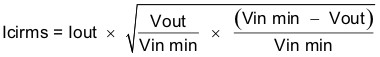
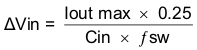
Table 1. Capacitor Types
| VENDOR | VALUE (μF) | EIA Size | VOLTAGE | DIALECTRIC | COMMENTS |
|---|---|---|---|---|---|
| Murata | 1.0 to 2.2 | 1210 | 100 V | X7R | GRM32 series |
| 1.0 to 4.7 | 50 V | ||||
| 1.0 | 1206 | 100 V | GRM31 series | ||
| 1.0 to 2.2 | 50 V | ||||
| Vishay | 1.0 10 1.8 | 2220 | 50 V | VJ X7R series | |
| 1.0 to 1.2 | 100 V | ||||
| 1.0 to 3.9 | 2225 | 50 V | |||
| 1.0 to 1.8 | 100 V | ||||
| TDK | 1.0 to 2.2 | 1812 | 100 V | C series C4532 | |
| 1.5 to 6.8 | 50 V | ||||
| 1.0. to 2.2 | 1210 | 100 V | C series C3225 | ||
| 1.0 to 3.3 | 50 V | ||||
| AVX | 1.0 to 4.7 | 1210 | 50 V | X7R dielectric series | |
| 1.0 | 100 V | ||||
| 1.0 to 4.7 | 1812 | 50 V | |||
| 1.0 to 2.2 | 100 V |
8.2.1.2.6 Slow-Start Capacitor
The slow-start capacitor determines the minimum amount of time it will take for the output voltage to reach its nominal programmed value during power-up. This is useful if a load requires a controlled voltage slew rate. This is also used if the output capacitance is large and would require large amounts of current to quickly charge the capacitor to the output voltage level. The large currents necessary to charge the capacitor may make the TPS54240 reach the current limit or excessive current draw from the input power supply may cause the input voltage rail to sag. Limiting the output voltage slew rate solves both of these problems.
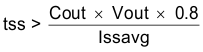
The slow-start time must be long enough to allow the regulator to charge the output capacitor up to the output voltage without drawing excessive current. Equation 40 can be used to find the minimum slow-start time, tss, necessary to charge the output capacitor, Cout, from 10% to 90% of the output voltage, Vout, with an average slow-start current of Issavg. In the example, to charge the effective output capacitance of 72.4 µF up to 3.3 V while only allowing the average output current to be 1 A would require a 0.19-ms slow-start time.
Once the slow-start time is known, the slow-start capacitor value can be calculated using Equation 6. For the example circuit, the slow-start time is not too critical since the output capacitor value is 2 x 47 μF which does not require much current to charge to 3.3 V. The example circuit has the slow start-time set to an arbitrary value of 3.5 ms which requires a 8.75 nF slow-start capacitor. For this design, the next larger standard value of 10 nF is used.
8.2.1.2.7 Bootstrap Capacitor Selection
A 0.1-μF ceramic capacitor must be connected between the BOOT and PH pins for proper operation. TI recommends using a ceramic capacitor with X5R or better grade dielectric. The capacitor should have a 10-V or higher voltage rating.
8.2.1.2.8 Undervoltage Lock Out Set Point
The Undervoltage Lock Out (UVLO) can be adjusted using an external voltage divider on the EN pin of the TPS54240. The UVLO has two thresholds, one for power-up when the input voltage is rising, and one for power-down or brown outs when the input voltage is falling. For the example design, the supply should turn on and start switching once the input voltage increases above 6.25 V (enabled). After the regulator starts switching, it should continue to do so until the input voltage falls below 5.9 V (UVLO stop).
The programmable UVLO and enable voltages are set using the resistor divider of R1 and R2 between Vin and ground to the EN pin. Equation 2 through Equation 3 can be used to calculate the resistance values necessary. For the example application, a 124 kΩ between Vin and EN (R1) and a 30.1 kΩ between EN and ground (R2) are required to produce the 6.25 and 5.9 volt start and stop voltages.
8.2.1.2.9 Output Voltage And Feedback Resistors Selection
The voltage divider of R5 and R6 is used to set the output voltage. For the example design, 10.0 kΩ was selected for R6. Using Equation 1, R5 is calculated as 31.25 kΩ. The nearest standard 1% resistor is 31.6 kΩ. Due to current leakage of the VSENSE pin, the current flowing through the feedback network should be greater than 1 μA to maintain the output voltage accuracy. This requirement makes the maximum value of R2 equal to 800 kΩ. Choosing higher resistor values will decrease quiescent current and improve efficiency at low-output currents but may introduce noise immunity problems.
8.2.1.2.10 Compensation
There are several methods used to compensate DC - DC regulators. The method presented here is easy to calculate and ignores the effects of the slope compensation that is internal to the device. Because the slope compensation is ignored, the actual cross-over frequency will usually be lower than the cross-over frequency used in the calculations. This method assumes the cross-over frequency is between the modulator pole and the ESR zero and the ESR zero is at least 10 times greater the modulator pole. Use SwitcherPro software for a more accurate design.
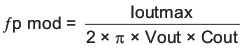
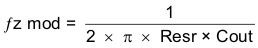
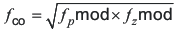
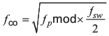
To get started, the modulator pole, fpmod, and the ESR zero, fz1 must be calculated using Equation 41 and Equation 42. For Cout, use a derated value of 40 μF. Use equations Equation 43 and Equation 44, to estimate a starting point for the crossover frequency, fco, to design the compensation. For the example design, fpmod is 1206 Hz and fzmod is 530.5 kHz. Equation 43 is the geometric mean of the modulator pole and the esr zero and Equation 44 is the mean of modulator pole and the switching frequency. Equation 43 yields 25.3 kHz and Equation 44 gives 13.4 kHz. Use the lower value of Equation 43 or Equation 44 for an initial crossover frequency. For this example, a higher fco is desired to improve transient response. the target fco is 35.0 kHz. Next, the compensation components are calculated. A resistor-in-series with a capacitor is used to create a compensating zero. A capacitor in parallel to these two components forms the compensating pole.
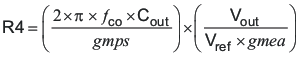
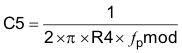
To determine the compensation resistor, R4, use Equation 45. Assume the power stage transconductance, gmps, is 10.5 A/V. The output voltage, Vo, reference voltage, VREF, and amplifier transconductance, gmea, are 3.3 V, 0.8 V and 310 μA/V, respectively. R4 is calculated to be 20.2 kΩ, use the nearest standard value of 20.0 kΩ. Use Equation 46 to set the compensation zero to the modulator pole frequency. Equation 46 yields 4740 pF for compensating capacitor C5, a 4700 pF is used for this design.
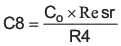
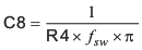
A compensation pole can be implemented if desired using an additional capacitor C8 in parallel with the series combination of R4 and C5. Use the larger value of Equation 47 and Equation 48 to calculate the C8, to set the compensation pole. C8 is not used for this design example.
8.2.1.2.11 Discontinuous Mode And Eco-Mode Boundary
With an input voltage of 12 V, the power supply enters discontinuous mode when the output current is less than 337 mA. The power supply enters Eco-Mode when the output current is lower than 5 mA.
The input current draw at no load is 392 μA.
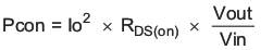
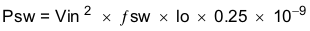
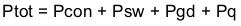
8.2.1.2.12 Power Dissipation Estimate
The following formulas show how to estimate the IC power dissipation under continuous conduction mode (CCM) operation. These equations should not be used if the device is working in discontinuous conduction mode (DCM).
The power dissipation of the IC includes conduction loss (Pcon), switching loss (Psw), gate drive loss (Pgd) and supply current (Pq).
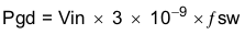
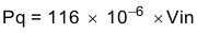
Where:
Iout is the output current (A).
RDS(on) is the on-resistance of the high-side MOSFET (Ω).
Vout is the output voltage (V).
Vin is the input voltage (V).
fsw is the switching frequency (Hz).
So
For given TA,

For given TJMAX = 150°C

Where:
Ptot is the total device power dissipation (W).
TA is the ambient temperature (°C).
TJ is the junction temperature (°C).
Rth is the thermal resistance of the package (°C/W).
TJMAX is maximum junction temperature (°C).
TAMAX is maximum ambient temperature (°C).
There will be additional power losses in the regulator circuit due to the inductor AC and DC losses, the catch diode and trace resistance that will impact the overall efficiency of the regulator.
8.2.1.3 Application Curves
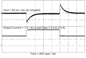 Figure 50. Load Transient
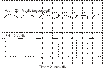 Figure 52. Output Ripple, CCM
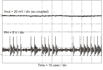 Figure 54. Output Ripple, PSM
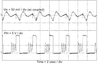 Figure 56. Input Ripple, DCM
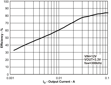 Figure 58. Light Load Efficiency
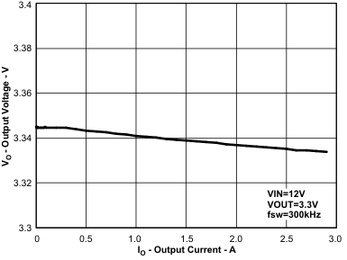 Figure 60. Regulation vs Load Current
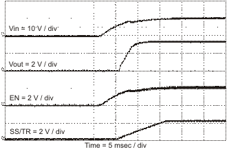 Figure 51. Startup With VIN
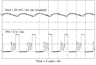 Figure 53. Output Ripple, DCM
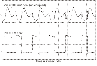 Figure 55. Input Ripple, CCM
 Figure 57. Efficiency vs Load Current
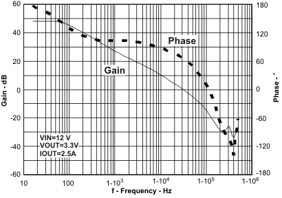 Figure 59. Overall Loop Frequency Response
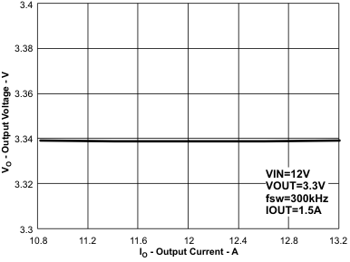 Figure 61. Regulation vs Input Voltage
8.2.2 TPS54240 Inverting Power Supply
This application circuit shows how to use the TPS54240 to convert a positive-input voltage to a negative-output voltage. Ideal applications are amplifiers requiring a negative power supply. For a more-detailed example, see Create an Inverting Power Supply From a Step-Down Regulator, application report SLVA317.
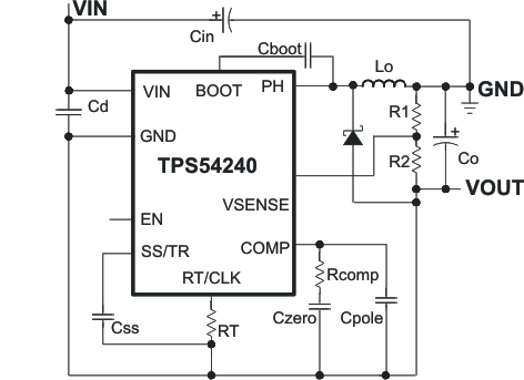 Figure 62. TPS54240 Inverting Power Supply
8.2.3 TPS54240 Split Rail Power Supply
This application circuit shows how to use the TPS54240 to convert a positive-input voltage to a split-rail positive- and negative-output voltage by using a coupled inductor. Ideal applications are amplifiers requiring a split-rail positive- and negative-voltage power supply. For a more-detailed example, see Creating a Split-Rail Power Supply With a Wide Input Voltage Buck Regulator, application report SLVA369.
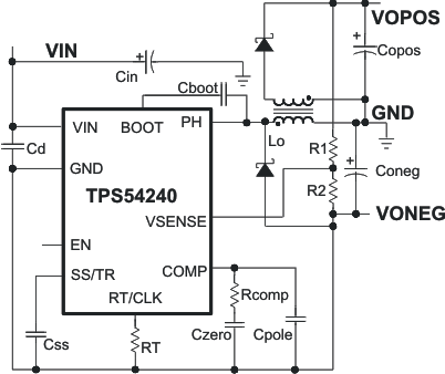 Figure 63. TPS54240 Split Rail Power Supply
8.2.4 12-V To 3.8-V GSM Power Supply
This application circuit is designed with TPS54240 device to power GSM-GPRS modules. GSM-GPRS modules typically require a power supply that can support large output current transients. For a more-detailed example, see Creating GSM-GPRS Power Supply, application report SLVA412.
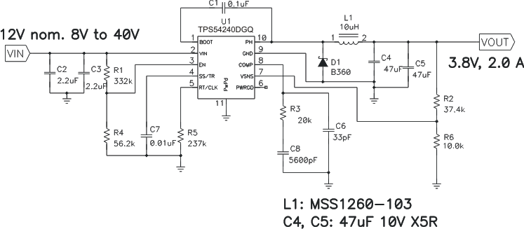 Figure 64. 12-V to 3.8-V GSM Power Supply
8.2.5 24-V to 4.2-V GSM Power Supply
This application circuit is also designed to power GSM-GPRS modules. For a more-detailed example, see Creating GSM-GPRS Power Supply, application report SLVA412.
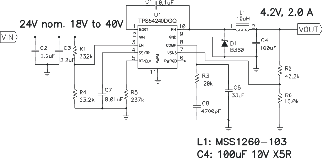 Figure 65. 24-V to 4.2-V GSM Power Supply