SLVSDG6B May 2016 – April 2021 TPS54302
PRODUCTION DATA
- 1 Features
- 2 Applications
- 3 Description
- 4 Revision History
- 5 Pin Configuration and Functions
- 6 Specifications
-
7 Detailed Description
- 7.1 Overview
- 7.2 Functional Block Diagram
- 7.3
Feature Description
- 7.3.1 Fixed-Frequency PWM Control
- 7.3.2 Pulse Skip Mode
- 7.3.3 Error Amplifier
- 7.3.4 Slope Compensation and Output Current
- 7.3.5 Enable and Adjusting Undervoltage Lockout
- 7.3.6 Safe Startup into Pre-Biased Outputs
- 7.3.7 Voltage Reference
- 7.3.8 Adjusting Output Voltage
- 7.3.9 Internal Soft-Start
- 7.3.10 Bootstrap Voltage (BOOT)
- 7.3.11 Overcurrent Protection
- 7.3.12 Spread Spectrum
- 7.3.13 Output Overvoltage Protection (OVP)
- 7.3.14 Thermal Shutdown
- 7.4 Device Functional Modes
- 8 Application and Implementation
- 9 Power Supply Recommendations
- 10Layout
- 11Device and Documentation Support
- 12Mechanical, Packaging, and Orderable Information
Package Options
Refer to the PDF data sheet for device specific package drawings
Mechanical Data (Package|Pins)
- DDC|6
Thermal pad, mechanical data (Package|Pins)
Orderable Information
8.2.3.5.3 Feedforward Capacitor
The TPS54302 device is internally compensated and the internal compensation network is composed of two capacitors and one resister shown on the Section 7.2. Depending on the VOUT, if the output capacitor COUT is dominated by low ESR (ceramic types) capacitors, it could result in low phase margin. To improve the phase boost an external feedforward capacitor C6 can be added in parallel with R2. The C6 capacitor is chosen such that phase margin is boosted at the crossover frequency.
Equation 16 for C6 was tested.
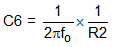
For this design, C6 = 75 pF. The C6 capacitor is not needed when COUT has high ESR, and C6 calculated from Equation 16 should be reduced with medium ESR. Table 8-2 can be used as a starting point.
Table 8-2 lists some recommended component values.
| VOUT (V) | L (µH) | COUT (µF) | R2 (kΩ) | R3 (kΩ) | C8 (pF) |
|---|---|---|---|---|---|
| 1.8 | 4.7 | 66 | 100 | 49.9 | 33 |
| 2.5 | 5.6 | 66 | 100 | 31.6 | 47 |
| 3.3 | 6.8 | 44 | 100 | 22.1 | 47 |
| 5 | 10 | 44 | 100 | 13.3 | 75 |
| 12 | 15 | 44 | 100 | 5.23 | 100 |