SLVS632K January 2006 – January 2024 TPS5430 , TPS5431
PRODUCTION DATA
- 1
- 1 Features
- 2 Applications
- 3 Description
- 4 Pin Configuration and Functions
- 5 Specifications
-
6 Detailed Description
- 6.1 Overview
- 6.2 Functional Block Diagram
- 6.3
Feature Description
- 6.3.1 Oscillator Frequency
- 6.3.2 Voltage Reference
- 6.3.3 Enable (ENA) and Internal Slow Start
- 6.3.4 Undervoltage Lockout (UVLO)
- 6.3.5 Boost Capacitor (BOOT)
- 6.3.6 Output Feedback (VSENSE) and Internal Compensation
- 6.3.7 Voltage Feed-Forward
- 6.3.8 Pulse-Width-Modulation (PWM) Control
- 6.3.9 Overcurrent Limiting
- 6.3.10 Overvoltage Protection
- 6.3.11 Thermal Shutdown
- 6.4 Device Functional Modes
-
7 Application and Implementation
- 7.1 Application Information
- 7.2
Typical Applications
- 7.2.1
12-V Input to 5.0-V Output
- 7.2.1.1 Design Requirements
- 7.2.1.2 Detailed Design Procedure
- 7.2.1.3 Application Curves
- 7.2.2 Wide Input Voltage Ranges with TPS5430
- 7.2.3 Circuit Using Ceramic Output Filter Capacitors
- 7.2.1
12-V Input to 5.0-V Output
- 7.3 Power Supply Recommendations
- 7.4 Layout
- 8 Device and Documentation Support
- 9 Revision History
- 10Mechanical, Packaging, and Orderable Information
Package Options
Refer to the PDF data sheet for device specific package drawings
Mechanical Data (Package|Pins)
- DDA|8
Thermal pad, mechanical data (Package|Pins)
Orderable Information
7.2.3.2.1 Output Filter Component Selection
Using Equation 11, the minimum inductor value is 12 μH. A value of 15 μH is chosen for this design.
When using ceramic output filer capacitors, the recommended LC resonant frequency must be no more than 7 kHz. Because the output inductor is already selected at 15 μH, this limits the minimum output capacitor value to:
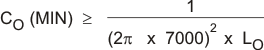
The minimum capacitor value is calculated to be 34 μF. For this circuit a larger value of capacitor yields better transient response. A single 100 μF output capacitor is used for C3. It is important to note that the actual capacitance of ceramic capacitors decreases with applied voltage. In this example, the output voltage is set to 3.3 V, minimizing this effect.