SLVS975C September 2009 – April 2018 TPS54318
PRODUCTION DATA.
- 1 Features
- 2 Applications
- 3 Description
- 4 Revision History
- 5 Pin Configuration and Functions
- 6 Specifications
-
7 Detailed Description
- 7.1 Overview
- 7.2 Functional Block Diagram
- 7.3
Feature Description
- 7.3.1 Fixed Frequency PWM Control
- 7.3.2 Slope Compensation and Output Current
- 7.3.3 Bootstrap Voltage (Boot) and Low Dropout Operation
- 7.3.4 Error Amplifier
- 7.3.5 Voltage Reference
- 7.3.6 Adjusting the Output Voltage
- 7.3.7 Enable and Adjusting Undervoltage Lockout
- 7.3.8 Soft-Start Pin
- 7.3.9 Sequencing
- 7.3.10 Constant Switching Frequency and Timing Resistor (RT/CLK Pin)
- 7.3.11 Overcurrent Protection
- 7.3.12 Frequency Shift
- 7.3.13 Reverse Overcurrent Protection
- 7.3.14 Synchronize Using the RT/CLK Pin
- 7.3.15 Power Good (PWRGD Pin)
- 7.3.16 Overvoltage Transient Protection
- 7.3.17 Thermal Shutdown
- 7.4 Device Functional Modes
-
8 Application and Implementation
- 8.1 Application Information
- 8.2
Typical Application
- 8.2.1 Design Requirements
- 8.2.2
Detailed Design Procedure
- 8.2.2.1 Step One: Select the Switching Frequency
- 8.2.2.2 Step Two: Select the Output Inductor
- 8.2.2.3 Step Three: Choose the Output Capacitor
- 8.2.2.4 Step Four: Select the Input Capacitor
- 8.2.2.5 Step Five: Minimum Load DC COMP Voltage
- 8.2.2.6 Step Six: Choose the Soft-Start Capacitor
- 8.2.2.7 Step Seven: Select the Bootstrap Capacitor
- 8.2.2.8 Step Eight: Undervoltage Lockout Threshold
- 8.2.2.9 Step Nine: Select Output Voltage and Feedback Resistors
- 8.2.2.10 Step 10: Select Loop Compensation Components
- 8.2.2.11 Power Dissipation Estimate
- 8.2.3 Application Curves
- 9 Power Supply Recommendations
- 10Layout
- 11Device and Documentation Support
- 12Mechanical, Packaging, and Orderable Information
Package Options
Mechanical Data (Package|Pins)
- RTE|16
Thermal pad, mechanical data (Package|Pins)
- RTE|16
Orderable Information
7.3.14 Synchronize Using the RT/CLK Pin
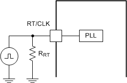
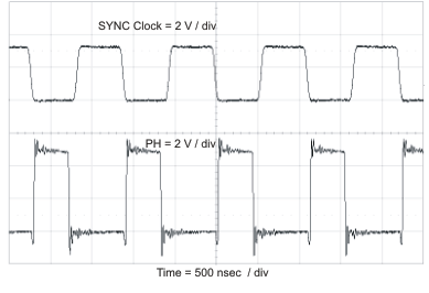
The RT/CLK pin is used to synchronize the converter to an external system clock. See Figure 29. To implement the synchronization feature in a system, connect a square wave to the RT/CLK pin with an on time of at least 75ns. If the pin is pulled above the PLL upper threshold, a mode change occurs and the pin becomes a synchronization input. The internal amplifier is disabled and the pin is a high impedance clock input to the internal PLL. If clocking edges stop, the internal amplifier is re-enabled and the mode returns to the frequency set by the resistor. The square wave amplitude at this pin must transition lower than 0.6 V and higher than 1.6 V typically. The recommended synchronization frequency range is 300 kHz to 2000 kHz. If the external system clock is to be removed, TI recommends that it be removed on the falling edge of the clock.

.
 Figure 30. Plot of Synchronizing to System Clock