SLUS774C AUGUST 2007 – December 2014 TPS54383 , TPS54386
PRODUCTION DATA.
- 1 Features
- 2 Applications
- 3 Description
- 4 Revision History
- 5 Pin Configuration and Functions
- 6 Specifications
-
7 Detailed Description
- 7.1 Overview
- 7.2 Functional Block Diagram
- 7.3
Feature Description
- 7.3.1 Voltage Reference
- 7.3.2 Oscillator
- 7.3.3 Input Undervoltage Lockout (UVLO) and Startup
- 7.3.4 Enable and Timed Turn On of the Outputs
- 7.3.5 Output Voltage Sequencing
- 7.3.6 Soft-Start
- 7.3.7 Output Voltage Regulation
- 7.3.8 Feedback Loop and Inductor-Capacitor (L-C) Filter Selection
- 7.3.9 Inductor-Capacitor (L-C) Selection
- 7.3.10 Maximum Output Capacitance
- 7.3.11 Minimum Output Capacitance
- 7.3.12 Modifying The Feedback Loop
- 7.3.13 Example: TPS54386 Buck Converter Operating at 12-V Input, 3.3-V Output and 400-mA(P-P) Ripple Current
- 7.3.14 Bootstrap for the N-Channel MOSFET
- 7.3.15 Light Load Operation
- 7.3.16 SW Node Ringing
- 7.3.17 Output Overload Protection
- 7.3.18 Operating Near Maximum Duty Cycle
- 7.3.19 Dual Supply Operation
- 7.3.20 Cascading Supply Operation
- 7.3.21 Multiphase Operation
- 7.3.22 Bypass and FIltering
- 7.3.23 Overtemperature Protection and Junction Temperature Rise
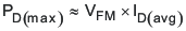
- 7.3.24 Power Derating
- 7.4 Device Functional Modes
-
8 Applications and Implementation
- 8.1 Application Information
- 8.2
Typical Applications
- 8.2.1
12-V to 5-V and 3.3-V Converter
- 8.2.1.1 Design Requirements
- 8.2.1.2
Detailed Design Procedure
- 8.2.1.2.1 Duty Cycle Estimation
- 8.2.1.2.2 Inductor Selection
- 8.2.1.2.3 Rectifier Diode Selection
- 8.2.1.2.4 Output Capacitor Selection
- 8.2.1.2.5 Voltage Setting
- 8.2.1.2.6 Compensation Capacitors
- 8.2.1.2.7 Input Capacitor Selection
- 8.2.1.2.8 Boot Strap Capacitor
- 8.2.1.2.9 ILIM
- 8.2.1.2.10 SEQ
- 8.2.1.2.11 Power Dissipation
- 8.2.1.3 Application Curves
- 8.2.2 24-V to 12-V and 24-V to 5-V
- 8.2.3 5-V to 3.3V and 5-V to 1.2 V
- 8.2.1
12-V to 5-V and 3.3-V Converter
- 9 Power Supply Recommendations
- 10Layout
- 11Device and Documentation Support
- 12Mechanical, Packaging, and Orderable Information
Package Options
Refer to the PDF data sheet for device specific package drawings
Mechanical Data (Package|Pins)
- PWP|14
Thermal pad, mechanical data (Package|Pins)
- PWP|14
Orderable Information
8 Applications and Implementation
NOTE
Information in the following applications sections is not part of the TI component specification, and TI does not warrant its accuracy or completeness. TI’s customers are responsible for determining suitability of components for their purposes. Customers should validate and test their design implementation to confirm system functionality.
8.1 Application Information
The TPS5438x is a dual 28-V, 3-A, step down regulator with an integrated high-side MOSFETs. This device is typically used to convert a higher DC voltage to a lower DC voltage with a maximum available output current of 3 A on each channel. Example applications are: High Density Point-of-Load Regulators for Set-top Box, Digital TV, Power for DSP and other Consumer Electronics.
8.2 Typical Applications
8.2.1 12-V to 5-V and 3.3-V Converter
The following example illustrates a design process and component selection for a 12-V to 5-V and 3.3-V dual non-synchronous buck regulator using the TPS54383 converter.
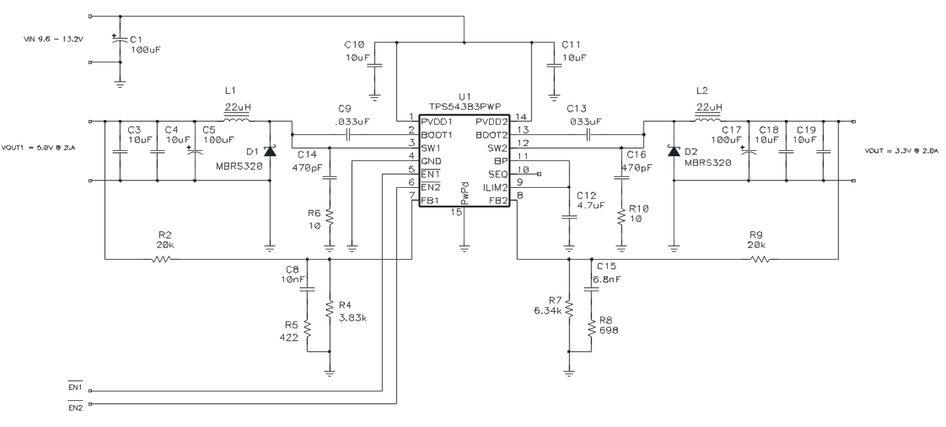 Figure 37. Design Example Schematic
8.2.1.1 Design Requirements
| PARAMETER | NOTES AND CONDITIONS | MIN | NOM | MAX | UNIT | |
|---|---|---|---|---|---|---|
| INPUT CHARACTERISTICS | ||||||
| VIN | Input voltage | 6.9 | 12.0 | 13.2 | V | |
| IIN | Input current | VIN = nom, IOUT = max | 1.6 | 2.0 | A | |
| No load input current | VIN = nom, IOUT = 0 A | 12 | 20 | mA | ||
| OUTPUT CHARACTERISTICS | ||||||
| VOUT1 | Output voltage 1 | VIN = nom, IOUT = nom | 4.8 | 5.0 | 5.2 | V |
| VOUT2 | Output voltage 2 | VIN = nom, IOUT = nom | 3.2 | 3.3 | 3.4 | |
| Line regulation | VIN = min to max | 1% | ||||
| Load regulation | IOUT = min to max | 1% | ||||
| VOUT(ripple) | Output voltage ripple | VIN = nom, IOUT = max | 50 | mVPP | ||
| IOUT1 | Output current 1 | VIN = min to max | 0 | 2.0 | A | |
| IOUT2 | Output current 2 | VIN = min to max | 0 | 2.0 | ||
| IOCP1 | Output overcurrent channel 1 | VIN = nom, VOUT = VOUT1 = 5% | 2.4 | 3 | 3.5 | |
| IOCP2 | Output overcurrent channel 2 | VIN = nom, VOUT = VOUT2 = 5% | 2.4 | 3 | 3.5 | |
| Transient response ΔVOUT from load transient | ΔIOUT = 1 A @ 3 A/μs | 200 | mV | |||
| Transient response settling time | 1 | ms | ||||
| SYSTEM CHARACTERISTICS | ||||||
| fSW | Switching frequency | 250 | 310 | 370 | kHz | |
| η | Full load efficiency | 85% | ||||
| TJ | Operating temperature range | 0 | 25 | 60 | °C | |
Table 3. Design Example List of Materials
| QTY | REFERENCE DESIGNATOR |
VALUE | DESCRIPTION | SIZE | PART NUMBER | MANUFACTURER |
|---|---|---|---|---|---|---|
| 1 | C1 | 100 μF | Capacitor, Aluminum, 25V, 20% | E-can | EEEFC1E101P | Panasonic |
| 2 | C10, C11 | 10 μF | Capacitor, Ceramic, 25V, X5R 20% | 1210 | C3216X5R1E106M | TDK |
| 1 | C12 | 4.7 μF | Capacitor, Ceramic, 10V, X5R 20% | 0805 | Std | Std |
| 2 | C14, C16 | 470 pF | Capacitor, Ceramic, 25V, X7R, 20% | 0603 | Std | Std |
| 1 | C15 | 6.8 nF | Capacitor, Ceramic, 25V, X7R, 20% | 0603 | Std | Std |
| 1 | C17, C5 | 100 μF | Capacitor, Aluminum, 10V, 20%, FC Series | F-can | EEEFC1A101P | Panasonic |
| 4 | C3, C4, C18, C19 | 10 μF | Capacitor, Ceramic, 6.3V, X5R 20% | 0805 | C2012X5R0J106M | TDK |
| 1 | C8 | 10 nF | Capacitor, Ceramic, 25V, X7R, 20% | 0603 | Std | Std |
| 2 | C9, C13 | 0.033 μF | Capacitor, Ceramic, 25V, X7R, 20% | 0603 | Std | Std |
| 2 | D1, D2 | MBRS320 | Diode, Schottky, 3-A, 30-V | SMC | MBRS330T3 | On Semi |
| 2 | L1, L2 | 22 μH | Inductor, Power, 6.8A, 0.038 Ω | 0.484 x 0.484 | MSS1278-153ML | Coilcraft |
| 2 | R2, R9 | 20 kΩ | Resistor, Chip, 1/16W, 1% | 0603 | Std | Std |
| 1 | R5 | 422 Ω | Resistor, Chip, 1/16W, 1% | 0603 | Std | Std |
| 2 | R6, R10 | 10 Ω | Resistor, Chip, 1/16W, 5% | 0603 | Std | Std |
| 1 | R8 | 698 Ω | Resistor, Chip, 1/16W, 1% | 0603 | Std | Std |
| 1 | R4 | 3.83 kΩ | Resistor, Chip, 1/16W, 1% | 0603 | Std | Std |
| 1 | R7 | 6.34 kΩ | Resistor, Chip, 1/16W, 1% | 0603 | Std | Std |
| 1 | U1 | TPS54383 DC-DC Switching Converter w/ FET | HTSSOP-14 | TPS54383PWP | TI |
8.2.1.2 Detailed Design Procedure
Use the following design procedure to select component values for the TPS5438x.
8.2.1.2.1 Duty Cycle Estimation
The first step is to estimate the duty cycle of each switching FET.
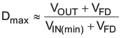
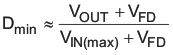
Using an assumed forward drop of 0.5 V for a schottky rectifier diode, the Channel 1 duty cycle is approximately 40.1% (minimum) to 48.7% (maximum) while the Channel 2 duty cycle is approximately 27.7% (minimum) to 32.2% (maximum).
8.2.1.2.2 Inductor Selection
The peak-to-peak ripple is limited to 30% of the maximum output current. This places the peak current far enough from the minimum overcurrent trip level to ensure reliable operation.
For both Channel 1 and Channel 2, the maximum inductor ripple current is 600 mA. The inductor size is estimated in Equation 23.
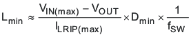
The inductor values are
- L1 = 18.3 μH
- L2 = 15.3 μH
The next higher standard inductor value of 22 μH is used for both inductors.
The resulting ripple currents are :
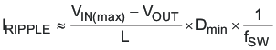
Peak-to-peak ripple currents of 0.498 A and 0.416 A are estimated for Channel 1 and Channel 2 respectively.
The RMS current through an inductor is approximated by Equation 25.
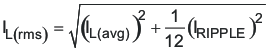
and is approximately 2.0 A for both channels.
The peak inductor current is found using:

An inductor with a minimum RMS current rating of 2.0 A and minimum saturation current rating of 2.25 A is required. A Coilcraft MSS1278-223ML 22-μH, 6.8-A inductor is selected.
8.2.1.2.3 Rectifier Diode Selection
A schottky diode is selected as a rectifier diode for its low forward voltage drop. Allowing 20% over VIN for ringing on the switch node, the required minimum reverse break-down voltage of the rectifier diode is:
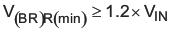
The diode must have reverse breakdown voltage greater than 15.8 V, therefore a 20-V device is used.
The average current in the rectifier diode is estimated by Equation 28.
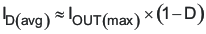
For this design, 1.2-A (average) and 2.25 A (peak) is estimated for Channel 1 and 1.5-A (average) and 2.21-A (peak) for Channel 2.
An MBRS320, 20-V, 3-A diode in an SMC package is selected for both channels. This diode has a forward voltage drop of 0.4 V at 2 A.
The power dissipation in the diode is estimated by Equation 29.
For this design, the full load power dissipation is estimated to be 480 mW in D1, and 580 mW in D2.
8.2.1.2.4 Output Capacitor Selection
The TPS54383's internal compensation limits the selection of the output capacitors. From Figure 25, the internal compensation has a double zero resonance at about 3 kHz. The output capacitor is selected by Equation 30.
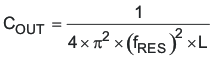
Solving for COUT using
- fRES = 3 kHz
- L = 22 μH
The resulting is COUT = 128 μF. The output ripple voltage of the converter is composed of the ripple voltage across the output capacitance and the ripple voltage across the ESR of the output capacitor. To find the maximum ESR allowable to meet the output ripple requirements the total ripple is partitioned, and the equation manipulated to find the ESR.
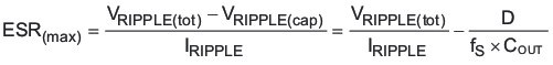
Based on 128 μF of capacitance, 300-kHz switching frequency and 50-mV ripple voltage plus rounding up the ripple current to 0.5 A, and the duty cycle to 50%, the capacitive portion of the ripple voltage is 6.5 mV, leaving a maximum allowable ESR of 87 mΩ.
To meet the ripple voltage requirements, a low-cost 100-μF electrolytic capacitor with 400 mΩ ESR (C5, C17) and two 10-μF ceramic capacitors (C3 and C4; and C18 and C19) with 2.5-mΩ ESR are selected. From the datasheets for the ceramic capacitors, the parallel combination provides an impedance of 28 mΩ @ 300 kHz for 14 mV of ripple.
8.2.1.2.5 Voltage Setting
The primary feedback divider resistors (R2, R9) from VOUT to FB should be between 10 kΩ and 50 kΩ to maintain a balance between power dissipation and noise sensitivity. For this design, 20 kΩ is selected.
The lower resistors, R4 and R7 are found using the following equations.
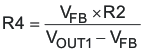
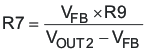
- R2 = R9 = 20 kΩ
- VFB = 0.80 V
- R4= 3.80 kΩ (3.83 kΩ standard value is used)
- R7= 6.40 kΩ (6.34 kΩ standard value is used)
8.2.1.2.6 Compensation Capacitors
Checking the ESR zero of the output capacitors:
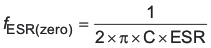
where
- C = 100 μF
- ESR = 400 mΩ
- ESR(zero) = 3980 Hz
Since the ESR zero of the main output capacitor is less than 20 kHz, an R-C filter is added in parallel with R4 and R7 to compensate for the electrolytic capacitors' ESR and add a zero approximately 40 kHz.
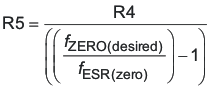
where
- fESR(zero) = 4 kHz
- fESR(desired) = 40 kHz
- R4 = 3.83 kΩ
- R5 = 424Ω (422Ω selected)
- R7 = 6.34 kΩ
- R8 = 702Ω (698Ω selected)
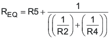
where
- R2 = R9 = 20 kΩ
- REQ1 = 3.63 kΩ
- REQ2 = 5.51 kΩ
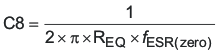
where
- C8 = 10.9 nF (10 nF selected)
- C15 = 7.22 nF (6800 pF selected)
8.2.1.2.7 Input Capacitor Selection
The TPS54383 datasheet recommends a minimum 10-μF ceramic input capacitor on each PVDD pin. These capacitor must be capable of handling the RMS ripple current of the converter. The RMS current in the input capacitors is estimated by Equation 38.
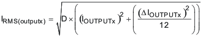
- IRMS(CIN) = 0.43 A
One 1210 10-μF, 25 V, X5R ceramic capacitor with 2-mΩ ESR and a 2-A RMS current rating are selected for each PVDD input. Higher voltage capacitors are selected to minimize capacitance loss at the DC bias voltage to ensure the capacitors maintain sufficient capacitance at the working voltage.
8.2.1.2.8 Boot Strap Capacitor
To ensure proper charging of the high-side FET gate and limit the ripple voltage on the boost capacitor, a 33-nF boot strap capacitor is used.
8.2.1.2.9 ILIM
Current limit must be set above the peak inductor current IL(peak). Comparing IL(peak) to the available minimum current limits, ILIM is connected to BP for the highest current limit level.
8.2.1.2.10 SEQ
The SEQ pin is left floating, leaving the enable pins to function independently. If the enable pins are tied together, the two supplies start-up ratiometrically. Alternatively, SEQ could be connected to BP or GND to provide sequential start-up.
8.2.1.2.11 Power Dissipation
The power dissipation in the TPS54383 is composed of FET conduction losses, switching losses and internal regulator losses. The RMS FET current is found using Equation 39.
This results in 1.05-A RMS for Channel 1 and 0.87-A RMS for Channel 2.
Conduction losses are estimated by:
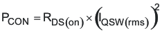
Conduction losses of 198 mW and 136 mW are estimated for Channel 1 and Channel 2 respectively.
The switching losses are estimated in Equation 41.
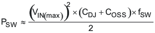
From the data sheet of the MBRS320, the junction capacitance is 658 pF. Since this is large compared to the output capacitance of the TPS54x8x the FET capacitance is neglected, leaving switching losses of 17 mW for each channel.
The regulator losses are estimated in Equation 42.

With no external load on BP (IBP=0) the regulator power dissipation is 66 mW.
Total power dissipation in the device is the sum of conduction and switching for both channels plus regulator losses.
The total power dissipation is PDISS=0.198+0.136+0.017+0.017+.066 = 434 mW.
8.2.1.3 Application Curves
The following results are from the TPS54383-001 EVM.
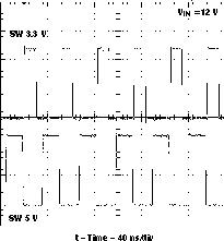 Figure 38. Switching Node Waveforms
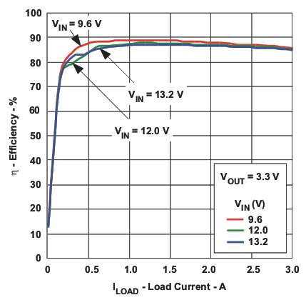 Figure 40. 3.3-V Output Efficiency vs. Load Current
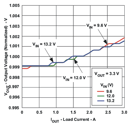 Figure 42. 3.3-V Output Voltage vs. Load Current
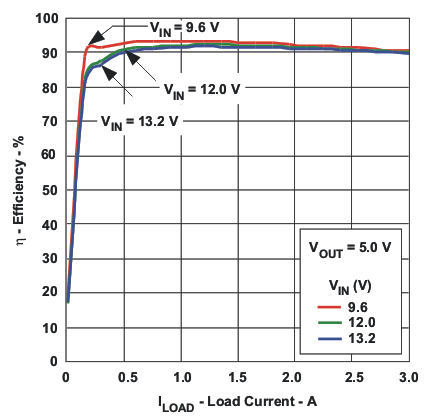 Figure 39. 5.0-V Output Efficiency vs. Load Current
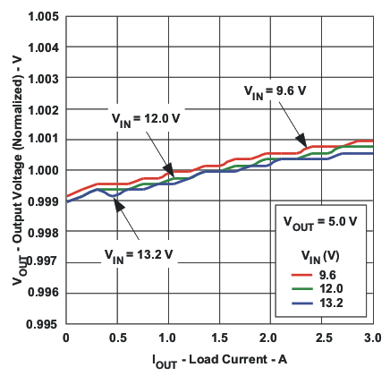 Figure 41. 5.0-V Output Voltage vs. Load Current
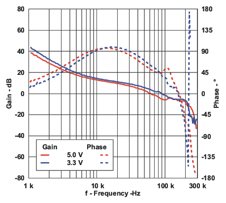 Figure 43. Example 1 Loop Response
8.2.2 24-V to 12-V and 24-V to 5-V
For a higher input voltage, both a snubber and bootstrap resistors are added to reduce ringing on the switch node and a 30 V schottky diode is selected. A higher resistance feedback network is chosen for the 12 V output to reduce the feedback current.
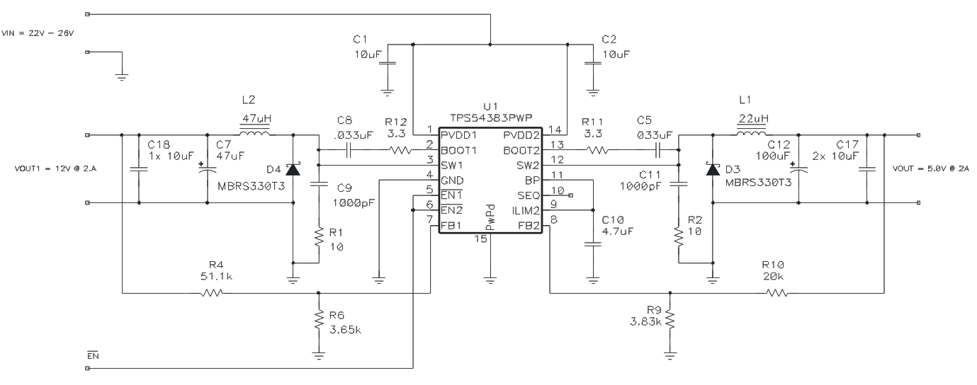 Figure 44. 24-V to 12-V and 24-V to 5-V Using the TPS54383
8.2.2.1 Design Requirements
| PARAMETER | NOTES AND CONDITIONS | MIN | NOM | MAX | UNIT | |
|---|---|---|---|---|---|---|
| INPUT CHARACTERISTICS | ||||||
| VIN | Input voltage | 22 | 24 | 26 | V | |
| OUTPUT CHARACTERISTICS | ||||||
| VOUT1 | Output voltage 1 | VIN = nom, IOUT = nom | 12.0 | V | ||
| VOUT2 | Output voltage 2 | VIN = nom, IOUT = nom | 5.0 | |||
| IOUT1 | Output current 1 | VIN = min to max | 0 | 2.0 | A | |
| IOUT2 | Output current 2 | VIN = min to max | 0 | 2.0 | ||
| SYSTEM CHARACTERISTICS | ||||||
| fSW | Switching frequency | 250 | 310 | 370 | kHz | |
8.2.2.2 Detailed Design Procedure
See the previous Detailed Design Procedure.
8.2.2.3 Application Curves
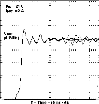 Figure 45. Switch Node Ringing Without Snubber and Boost Resistor
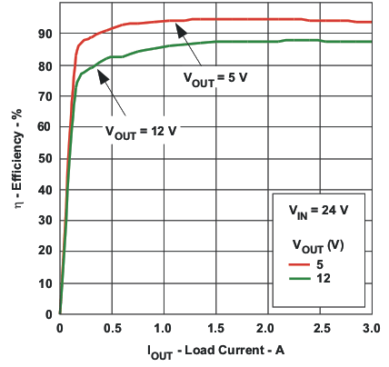 Figure 47. Efficiency vs. Load Current
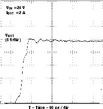 Figure 46. Switch Node Ringeing With Snubber and Boost Resistor
8.2.3 5-V to 3.3V and 5-V to 1.2 V
For a low input voltage application, the TPS54386 is selected for reduced size and all ceramic output capacitors are used. 22-μF input capacitors are selected to reduce input ripple and lead capacitors are placed in the feedback to boost phase margin.
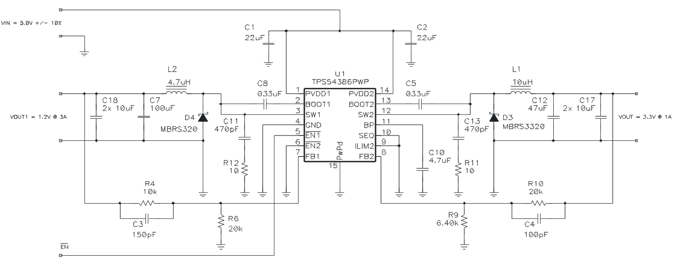 Figure 48. 5-V to 3.3V and 5-V to 1.2 V
8.2.3.1 Design Requirements
| PARAMETER | NOTES AND CONDITIONS | MIN | NOM | MAX | UNIT | |
|---|---|---|---|---|---|---|
| INPUT CHARACTERISTICS | ||||||
| VIN | Input voltage | 4.75 | 5 | 5.25 | V | |
| OUTPUT CHARACTERISTICS | ||||||
| VOUT1 | Output voltage 1 | VIN = nom, IOUT = nom | 1,2 | V | ||
| VOUT2 | Output voltage 2 | VIN = nom, IOUT = nom | 3.3 | |||
| IOUT1 | Output current 1 | VIN = min to max | 0 | 3 | A | |
| IOUT2 | Output current 2 | VIN = min to max | 0 | 1 | ||
| SYSTEM CHARACTERISTICS | ||||||
| fSW | Switching frequency | 510 | 630 | 750 | kHz | |
8.2.3.2 Detailed Design Procedure
See the pervious Detailed Design Procedure and Using All Ceramic Output Capacitors.
8.2.3.3 Application Curves
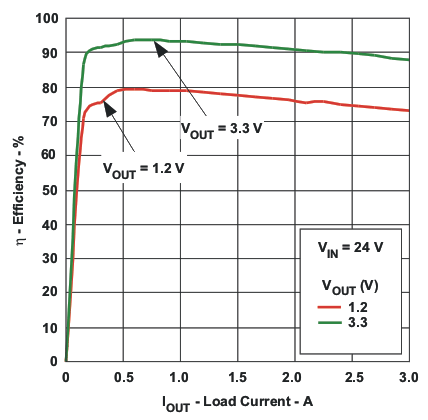 Figure 49. Efficiency vs. Load Current
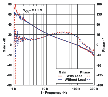 Figure 50. Example 3 Loop Response