SLUS774C AUGUST 2007 – December 2014 TPS54383 , TPS54386
PRODUCTION DATA.
- 1 Features
- 2 Applications
- 3 Description
- 4 Revision History
- 5 Pin Configuration and Functions
- 6 Specifications
-
7 Detailed Description
- 7.1 Overview
- 7.2 Functional Block Diagram
- 7.3
Feature Description
- 7.3.1 Voltage Reference
- 7.3.2 Oscillator
- 7.3.3 Input Undervoltage Lockout (UVLO) and Startup
- 7.3.4 Enable and Timed Turn On of the Outputs
- 7.3.5 Output Voltage Sequencing
- 7.3.6 Soft-Start
- 7.3.7 Output Voltage Regulation
- 7.3.8 Feedback Loop and Inductor-Capacitor (L-C) Filter Selection
- 7.3.9 Inductor-Capacitor (L-C) Selection
- 7.3.10 Maximum Output Capacitance
- 7.3.11 Minimum Output Capacitance
- 7.3.12 Modifying The Feedback Loop
- 7.3.13 Example: TPS54386 Buck Converter Operating at 12-V Input, 3.3-V Output and 400-mA(P-P) Ripple Current
- 7.3.14 Bootstrap for the N-Channel MOSFET
- 7.3.15 Light Load Operation
- 7.3.16 SW Node Ringing
- 7.3.17 Output Overload Protection
- 7.3.18 Operating Near Maximum Duty Cycle
- 7.3.19 Dual Supply Operation
- 7.3.20 Cascading Supply Operation
- 7.3.21 Multiphase Operation
- 7.3.22 Bypass and FIltering
- 7.3.23 Overtemperature Protection and Junction Temperature Rise
- 7.3.24 Power Derating
- 7.4 Device Functional Modes
-
8 Applications and Implementation
- 8.1 Application Information
- 8.2
Typical Applications
- 8.2.1
12-V to 5-V and 3.3-V Converter
- 8.2.1.1 Design Requirements
- 8.2.1.2
Detailed Design Procedure
- 8.2.1.2.1 Duty Cycle Estimation
- 8.2.1.2.2 Inductor Selection
- 8.2.1.2.3 Rectifier Diode Selection
- 8.2.1.2.4 Output Capacitor Selection
- 8.2.1.2.5 Voltage Setting
- 8.2.1.2.6 Compensation Capacitors
- 8.2.1.2.7 Input Capacitor Selection
- 8.2.1.2.8 Boot Strap Capacitor
- 8.2.1.2.9 ILIM
- 8.2.1.2.10 SEQ
- 8.2.1.2.11 Power Dissipation
- 8.2.1.3 Application Curves
- 8.2.2 24-V to 12-V and 24-V to 5-V
- 8.2.3 5-V to 3.3V and 5-V to 1.2 V
- 8.2.1
12-V to 5-V and 3.3-V Converter
- 9 Power Supply Recommendations
- 10Layout
- 11Device and Documentation Support
- 12Mechanical, Packaging, and Orderable Information
Package Options
Refer to the PDF data sheet for device specific package drawings
Mechanical Data (Package|Pins)
- PWP|14
Thermal pad, mechanical data (Package|Pins)
- PWP|14
Orderable Information
5 Pin Configuration and Functions
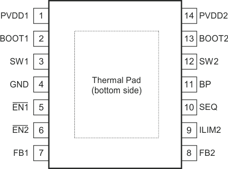
Pin Functions
| PIN | I/O | DESCRIPTION | |
|---|---|---|---|
| NAME | NO. | ||
| BOOT1 | 2 | I | Input supply to the high side gate driver for Output 1. Connect a 22-nF to 82-nF capacitor from this pin to SW1. This capacitor is charged from the BP pin voltage through an internal switch. The switch is turned ON during the OFF time of the converter. To slow down the turn ON of the internal FET, a small resistor (1 Ω to 3 Ω) may be placed in series with the bootstrap capacitor. |
| BOOT2 | 13 | I | Input supply to the high side gate driver for Output 2. Connect a 22-nF to 82-nF capacitor from this pin to SW2. This capacitor is charged from the BP pin voltage through an internal switch. The switch is turned ON during the OFF time of the converter. To slow down the turn ON of the internal FET, a small resistor (1 Ω to 3 Ω) may be placed in series with the bootstrap capacitor. |
| BP | 11 | - | Regulated voltage to charge the bootstrap capacitors. Bypass this pin to GND with a low ESR (4.7-μF to 10-μF X7R or X5R) ceramic capacitor. |
| EN1 | 5 | I | Active low enable input for Output 1. If the voltage on this pin is greater than 1.55 V, Output 1 is disabled (high-side switch is OFF). A voltage of less than 0.9 V enables Output 1 and allows soft-start of Output 1 to begin. An internal current source drives this pin to PVDD2 if left floating. Connect this pin to GND for "always ON" operation. |
| EN2 | 6 | I | Active low enable input for Output 2. If the voltage on this pin is greater than 1.55 V, Output 2 is disabled (high-side switch is OFF). A voltage of less than 0.9 V enables Output 2 and allows soft-start of Output 2 to begin. An internal current source drives this pin to PVDD2 if left floating. Connect this pin to GND for "always ON" operation. |
| FB1 | 7 | I | Voltage feedback pin for Output 1. The internal transconductance error amplifier adjusts the PWM for Output 1 to regulate the voltage at this pin to the internal 0.8-V reference. A series resistor divider from Output 1 to ground, with the center connection tied to this pin, determines the value of the regulated output voltage. Compensation for the feedback loop is provided internally to the device. See Feedback Loop and Inductor-Capacitor ( L-C) Filter Selection section for further information. |
| FB2 | 8 | I | Voltage feedback pin for Output 2. The internal transconductance error amplifier adjusts the PWM for Output 2 to regulate the voltage at this pin to the internal 0.8-V reference. A series resistor divider from Output 2 to ground, with the center connection tied to this pin, determines the value of the regulated Output voltage. Compensation for the feedback loop is provided internally to the device. See Feedback Loop and Inductor-Capacitor ( L-C) Filter Selection section for further information. |
| GND | 4 | - | Ground pin for the device. Connect directly to Thermal Pad. |
| ILIM2 | 9 | I | Current limit adjust pin for Output 2 only. This function is intended to allow a user with asymmetrical load currents (Output 1 load current much greater than Output 2 load current) to optimize component scaling of the lower current output while maintaining proper component derating in a overcurrent fault condition. The discrete levels are available as shown in Table 2. Note: An internal 2-resistor divider (150-kΩ each) connects BP to ILIM2 and to GND. |
| PVDD1 | 1 | I | Power input to the Output 1 high side MOSFET only. This pin should be locally bypassed to GND with a low ESR ceramic capacitor of 10-μF or greater. |
| PVDD2 | 14 | I | The PVDD2 pin provides power to the device control circuitry, provides the pull-up for the EN1 and EN2 pins and provides power to the Output 2 high-side MOSFET. This pin should be locally bypassed to GND with a low ESR ceramic capacitor of 10-μF or greater. The UVLO function monitors PVDD2 and enables the device when PVDD2 is greater than 4.1 V. |
| SEQ | 10 | I | This pin configures the output startup mode. If the SEQ pin is connected to BP, then when Output 2 is enabled, Output 1 is allowed to start after Output 2 has reached regulation; that is, sequential startup where Output 1 is slave to Output 2. If EN2 is allowed to go high after the outputs have been operating, then both outputs are disabled immediately, and the output voltages decay according to the load that is present. For this sequence configuration, tie EN1 to ground. If the SEQ pin is connected to GND, then when Output 1 is enabled, Output 2 is allowed to start after Output 1 has reached regulation; that is, sequential startup where Output 2 is slave to Output 1. If EN1 is allowed to go high after the outputs have been operating, then both outputs are disabled immediately, and the output voltages decay according to the load that is present. For this sequence configuration, tie EN2 to ground. If left floating, Output 1 and Output 2 start ratio-metrically when both outputs are enabled at the same time. They will soft-start at a rate determined by their final output voltage and enter regulation at the same time. If the EN1 and EN2 pins are allowed to operate independently, then the two outputs also operate independently NOTE: An internal two resistor (150-kΩ each) divider connects BP to SEQ and to GND. See the Sequence States table. |
| SW1 | 3 | O | Source (switching) output for Output 1 PWM. A snubber is recommended to reduce ringing on this node. See SW Node Ringing for further information. |
| SW2 | 12 | O | Source (switching) output for Output 2 PWM. A snubber is recommended to reduce ringing on this node. See SW Node Ringing for further information. |
| Thermal Pad | — | — | This pad must be tied externally to a ground plane and the GND pin. |