SLVSBZ0A September 2013 – December 2014 TPS54560-Q1
PRODUCTION DATA.
- 1 Features
- 2 Applications
- 3 Description
- 4 Revision History
- 5 Pin Configuration and Functions
- 6 Specifications
-
7 Detailed Description
- 7.1 Overview
- 7.2 Functional Block Diagram
- 7.3
Feature Description
- 7.3.1 Fixed Frequency PWM Control
- 7.3.2 Slope Compensation Output Current
- 7.3.3 Pulse Skip Eco-Mode
- 7.3.4 Low Dropout Operation and Bootstrap Voltage (BOOT)
- 7.3.5 Error Amplifier
- 7.3.6 Adjusting the Output Voltage
- 7.3.7 Enable and Adjusting Undervoltage Lockout
- 7.3.8 Internal Soft-Start
- 7.3.9 Constant Switching Frequency and Timing Resistor (RT/CLK) Pin)
- 7.3.10 Accurate Current Limit Operation and Maximum Switching Frequency
- 7.3.11 Synchronization to RT/CLK Pin
- 7.3.12 Overvoltage Protection
- 7.3.13 Thermal Shutdown
- 7.3.14 Small Signal Model for Loop Response
- 7.3.15 Simple Small Signal Model for Peak Current Mode Control
- 7.3.16 Small Signal Model for Frequency Compensation
- 7.4 Device Functional Modes
-
8 Applications and Implementation
- 8.1 Application Information
- 8.2
Typical Application
- 8.2.1 Design Requirements
- 8.2.2
Detailed Design Procedure
- 8.2.2.1 Selecting the Switching Frequency
- 8.2.2.2 Output Inductor Selection (LO)
- 8.2.2.3 Output Capacitor
- 8.2.2.4 Catch Diode
- 8.2.2.5 Input Capacitor
- 8.2.2.6 Bootstrap Capacitor Selection
- 8.2.2.7 Undervoltage Lockout Set Point
- 8.2.2.8 Output Voltage and Feedback Resistors Selection
- 8.2.2.9 Compensation
- 8.2.2.10 Discontinuous Conduction Mode and Eco-Mode Boundary
- 8.2.3 Application Curves
- 9 Power Supply Recommendations
- 10Layout
- 11Device and Documentation Support
- 12Mechanical, Packaging, and Orderable Information
Package Options
Mechanical Data (Package|Pins)
- DDA|8
Thermal pad, mechanical data (Package|Pins)
- DDA|8
Orderable Information
10 Layout
10.1 Layout Guidelines
Layout is a critical portion of good power supply design. There are several signal paths that conduct fast changing currents or voltages that can interact with stray inductance or parasitic capacitance to generate noise or degrade performance. To reduce parasitic effects, the VIN pin should be bypassed to ground with a low ESR ceramic bypass capacitor with X5R or X7R dielectric. Care should be taken to minimize the loop area formed by the bypass capacitor connections, the VIN pin, and the A node of the catch diode. See Figure 57 for a PCB layout example. The GND pin should be tied directly to the power pad under the IC and the power pad.
The power pad should be connected to internal PCB ground planes using multiple vias directly under the IC. The SW pin should be routed to the cathode of the catch diode and to the output inductor. Since the SW connection is the switching node, the catch diode and output inductor should be located close to the SW pins, and the area of the PCB conductor minimized to prevent excessive capacitive coupling. For operation at full rated load, the top side ground area must provide adequate heat dissipating area. The RT/CLK pin is sensitive to noise so the RT resistor should be located as close as possible to the IC and routed with minimal lengths of trace. The additional external components can be placed approximately as shown. It may be possible to obtain acceptable performance with alternate PCB layouts, however this layout has been shown to produce good results and is meant as a guideline.
10.2 Layout Example
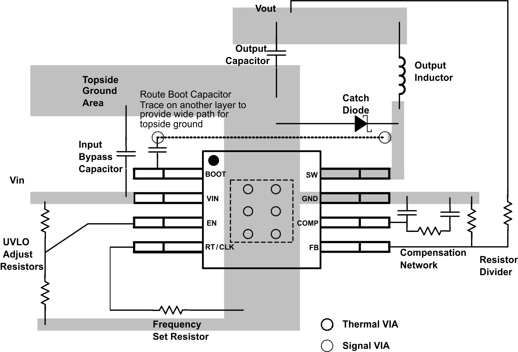 Figure 57. PCB Layout Example
10.3 Power Dissipation
The following formulas show how to estimate the TPS54560-Q1 power dissipation under continuous conduction mode (CCM) operation. These equations should not be used if the device is operating in discontinuous conduction mode (DCM).
The power dissipation of the IC includes conduction loss (PCOND), switching loss (PSW), gate drive loss (PGD) and supply current (PQ). Example calculations are shown with the 12 V typical input voltage of the design example.


Where:
IOUT is the output current (A).
RDS(on) is the on-resistance of the high-side MOSFET (Ω).
VOUT is the output voltage (V).
VIN is the input voltage (V).
fsw is the switching frequency (Hz).
trise is the SW pin voltage rise time and can be estimated by trise = VIN x 0.16 ns/V + 3 ns
QG is the total gate charge of the internal MOSFET
IQ is the operating nonswitching supply current
Therefore,

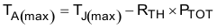
For given TA,
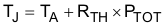
For given TJMAX = 150°C
Where:
Ptot is the total device power dissipation (W).
TA is the ambient temperature (°C).
TJ is the junction temperature (°C).
RTH is the thermal resistance of the package (°C/W).
TJMAX is maximum junction temperature (°C).
TAMAX is maximum ambient temperature (°C).
There will be additional power losses in the regulator circuit due to the inductor ac and dc losses, the catch diode and PCB trace resistance impacting the overall efficiency of the regulator.
10.4 Safe Operating Area
The safe operating area (SOA) of the device is shown in Figure 58, through Figure 61 for 3.3 V, 5 V and 12 V outputs and varying amounts of forced air flow. The temperature derating curves represent the conditions at which the internal components are at or below the manufacturer’s maximum operating temperatures. Derating limits apply to devices soldered directly to a double-sided PCB with 2 oz. copper, similar to the EVM. Careful attention must be paid to the other components chosen for the design, especially the catch diode.
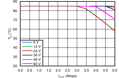 Figure 58. 3.3-V Outputs
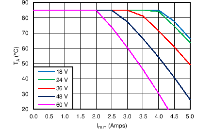 Figure 60. 12-V Outputs
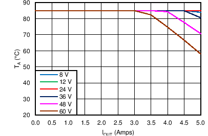 Figure 59. 5-V Outputs
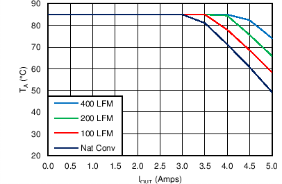 Figure 61. Air Flow Conditions
VIN = 36 V, VO = 12 V