SLVSBZ0A September 2013 – December 2014 TPS54560-Q1
PRODUCTION DATA.
- 1 Features
- 2 Applications
- 3 Description
- 4 Revision History
- 5 Pin Configuration and Functions
- 6 Specifications
-
7 Detailed Description
- 7.1 Overview
- 7.2 Functional Block Diagram
- 7.3
Feature Description
- 7.3.1 Fixed Frequency PWM Control
- 7.3.2 Slope Compensation Output Current
- 7.3.3 Pulse Skip Eco-Mode
- 7.3.4 Low Dropout Operation and Bootstrap Voltage (BOOT)
- 7.3.5 Error Amplifier
- 7.3.6 Adjusting the Output Voltage
- 7.3.7 Enable and Adjusting Undervoltage Lockout
- 7.3.8 Internal Soft-Start
- 7.3.9 Constant Switching Frequency and Timing Resistor (RT/CLK) Pin)
- 7.3.10 Accurate Current Limit Operation and Maximum Switching Frequency
- 7.3.11 Synchronization to RT/CLK Pin
- 7.3.12 Overvoltage Protection
- 7.3.13 Thermal Shutdown
- 7.3.14 Small Signal Model for Loop Response
- 7.3.15 Simple Small Signal Model for Peak Current Mode Control
- 7.3.16 Small Signal Model for Frequency Compensation
- 7.4 Device Functional Modes
-
8 Applications and Implementation
- 8.1 Application Information
- 8.2
Typical Application
- 8.2.1 Design Requirements
- 8.2.2
Detailed Design Procedure
- 8.2.2.1 Selecting the Switching Frequency
- 8.2.2.2 Output Inductor Selection (LO)
- 8.2.2.3 Output Capacitor
- 8.2.2.4 Catch Diode
- 8.2.2.5 Input Capacitor
- 8.2.2.6 Bootstrap Capacitor Selection
- 8.2.2.7 Undervoltage Lockout Set Point
- 8.2.2.8 Output Voltage and Feedback Resistors Selection
- 8.2.2.9 Compensation
- 8.2.2.10 Discontinuous Conduction Mode and Eco-Mode Boundary
- 8.2.3 Application Curves
- 9 Power Supply Recommendations
- 10Layout
- 11Device and Documentation Support
- 12Mechanical, Packaging, and Orderable Information
Package Options
Mechanical Data (Package|Pins)
- DDA|8
Thermal pad, mechanical data (Package|Pins)
- DDA|8
Orderable Information
5 Pin Configuration and Functions
DDA Package
8-Pin HSOIC
Top View
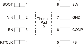
Pin Functions
| PIN | I/O | DESCRIPTION | ||
|---|---|---|---|---|
| NAME | NO. | |||
| BOOT | 1 | O | A bootstrap capacitor is required between BOOT and SW. If the voltage on this capacitor is below the minimum required to operate the high-side MOSFET, the output is switched off until the capacitor is refreshed. | |
| VIN | 2 | I | Input supply voltage with 4.5 V to 60 V operating range. | |
| EN | 3 | I | Enable pin, with internal pull-up current source. Pull below 1.2 V to disable. Float to enable. Adjust the input undervoltage lockout with two resistors. See the Enable and Adjusting Undervoltage Lockout section. | |
| RT/CLK | 4 | I | Resistor Timing and External Clock. An internal amplifier holds this pin at a fixed voltage when using an external resistor to ground to set the switching frequency. If the pin is pulled above the PLL upper threshold, a mode change occurs and the pin becomes a synchronization input. The internal amplifier is disabled and the pin is a high impedance clock input to the internal PLL. If clocking edges stop, the internal amplifier is re-enabled and the operating mode returns to resistor frequency programming. | |
| FB | 5 | I | Inverting input of the transconductance (gm) error amplifier. | |
| COMP | 6 | O | Error amplifier output and input to the output switch current (PWM) comparator. Connect frequency compensation components to this pin. | |
| GND | 7 | – | Ground | |
| SW | 8 | I | The source of the internal high-side power MOSFET and switching node of the converter. | |
| Thermal Pad | 9 | – | GND pin must be electrically connected to the exposed pad on the printed circuit board for proper operation. | |