SLVS400D August 2001 – January 2015 TPS54611 , TPS54612 , TPS54613 , TPS54614 , TPS54615 , TPS54616
PRODUCTION DATA.
- 1 Features
- 2 Applications
- 3 Description
- 4 Revision History
- 5 Pin Configuration and Functions
- 6 Specifications
-
7 Detailed Description
- 7.1 Overview
- 7.2 Functional Block Diagram
- 7.3
Feature Description
- 7.3.1 Undervoltage Lock Out (UVLO)
- 7.3.2 Slow-Start and Enable (SS/ENA)
- 7.3.3 VBIAS Regulator
- 7.3.4 Voltage Reference
- 7.3.5 Oscillator and PWM Ramp
- 7.3.6 Error Amplifier
- 7.3.7 PWM Control
- 7.3.8 Dead-Time Control and MOSFET Drivers
- 7.3.9 Overcurrent Protection
- 7.3.10 Thermal Shutdown
- 7.3.11 Powergood (PWRGD)
- 7.4 Device Functional Modes
- 8 Application and Implementation
- 9 Power Supply Recommendations
- 10Layout
- 11Device and Documentation Support
- 12Mechanical, Packaging, and Orderable Information
Package Options
Mechanical Data (Package|Pins)
- PWP|28
Thermal pad, mechanical data (Package|Pins)
- PWP|28
Orderable Information
8 Application and Implementation
NOTE
Information in the following applications sections is not part of the TI component specification, and TI does not warrant its accuracy or completeness. TI’s customers are responsible for determining suitability of components for their purposes. Customers should validate and test their design implementation to confirm system functionality.
8.1 Application Information
The TPS5461x devices are fixed output voltage synchronous step-down DC-DC converters. These devices are used to convert a higher DC input voltage to a lower DC output voltage with a maximum output current of 6A.
8.2 Typical Application
Figure 10 shows the schematic diagram for a typical TPS54614 application. The TPS54614 (U1) can provide greater than 6 A of output current at a nominal output voltage of 1.8 V. For proper operation, the exposed thermal PowerPAD underneath the integrated circuit package needs to be soldered to the printed-circuit board.
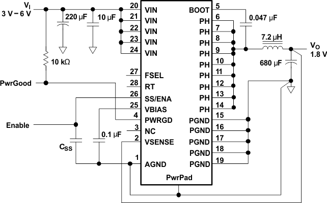 Figure 10. Application Circuit
8.2.1 Design Requirements
The design requirements for this example are listed in Table 3.
Table 3. Design Parameters
| DESIGN PARAMETER | EXAMPLE VALUE | |||
|---|---|---|---|---|
| DC Input Voltage Range | 3 V – 6 V | |||
| DC Output Voltage | 1 V | |||
| DC Output Current Range | 0A – 6 A | |||
| Load Transient Step | 3A – 6 A | |||
| Load Regulation Control | ± 5 mV | |||
| Loop Crossover Frequency | 50 kHz | |||
| Control Loop Phase Margin | 55° | |||
8.2.2 Detailed Design Procedure
8.2.2.1 Component Selection
The values for the components used in this design example were selected using the SWIFT designer software tool. SWIFT designer provides a complete design environment for developing dc-dc converters using the TPS54614, or other devices in the SWIFT product family. Additional design information is available at www.ti.com.
8.2.2.2 Input Filter
The input to the circuit is a nominal 3.3 VDC or 5 VDC. The input filter is a 220-μF POSCAP capacitor, with a maximum allowable ripple current of 3 A. A 10-µF ceramic capacitor for the TPS54614 is required, and must be located as close as possible to the device.
8.2.2.3 Feedback Circuit
The output voltage of the converter is fed directly into the VSENSE pin of the TPS54614. The TPS54614 is internally compensated to provide stability of the output under varying line and load conditions.
8.2.2.4 Operating Frequency
In the application circuit, 350 kHz operation is selected by leaving FSEL open. Different operating frequencies can be selected by connecting a resistor between RT pin and AGND. Choose the value of R using Equation 4 for the desired operating frequency:
Alternately, a preset operating frequency of 550 kHz can be selected by leaving RT open and connecting the FSEL pin to VI.
8.2.2.5 Output Filter
The output filter is composed of a 5.2-µH inductor and a 470-µF capacitor. The inductor is low dc resistance (16-mΩ) type, Sumida CDRH104R−5R2. The capacitor used is a 4-V POSCAP with a maximum ESR of 40 mΩ. The output filter components work with the internal compensation network to provide a stable closed loop response for the converter.
8.2.3 Application Curves
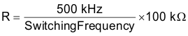
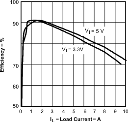 Figure 11. Efficiency vs Load Current
 Figure 13. Loop Response
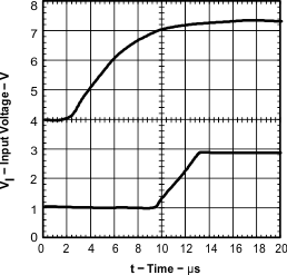 Figure 15. Start-up Waveforms
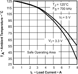 Figure 17. Ambient Temperature vs Load Current
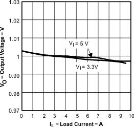 Figure 12. Output Voltage vs Load Current
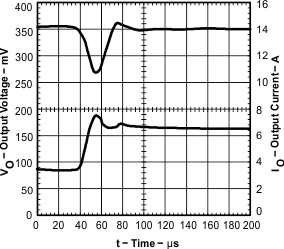 Figure 14. Transient Response
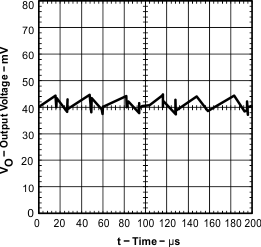 Figure 16. Output Ripple Voltage