SLVS400D August 2001 – January 2015 TPS54611 , TPS54612 , TPS54613 , TPS54614 , TPS54615 , TPS54616
PRODUCTION DATA.
- 1 Features
- 2 Applications
- 3 Description
- 4 Revision History
- 5 Pin Configuration and Functions
- 6 Specifications
-
7 Detailed Description
- 7.1 Overview
- 7.2 Functional Block Diagram
- 7.3
Feature Description
- 7.3.1 Undervoltage Lock Out (UVLO)
- 7.3.2 Slow-Start and Enable (SS/ENA)
- 7.3.3 VBIAS Regulator
- 7.3.4 Voltage Reference
- 7.3.5 Oscillator and PWM Ramp
- 7.3.6 Error Amplifier
- 7.3.7 PWM Control
- 7.3.8 Dead-Time Control and MOSFET Drivers
- 7.3.9 Overcurrent Protection
- 7.3.10 Thermal Shutdown
- 7.3.11 Powergood (PWRGD)
- 7.4 Device Functional Modes
- 8 Application and Implementation
- 9 Power Supply Recommendations
- 10Layout
- 11Device and Documentation Support
- 12Mechanical, Packaging, and Orderable Information
Package Options
Mechanical Data (Package|Pins)
- PWP|28
Thermal pad, mechanical data (Package|Pins)
- PWP|28
Orderable Information
10 Layout
10.1 Layout Guidelines
Figure 18 shows a generalized PCB layout guide for the TPS5461x.
- The VIN pins should be connected together on the printed circuit board (PCB) and bypassed with a low ESR ceramic bypass capacitor. Care should be taken to minimize the loop area formed by the bypass capacitor connections, the VIN pins, and the TPS54311−16 ground pins. The minimum recommended bypass capacitance is 10-μF ceramic with a X5R or X7R dielectric and the optimum placement is closest to the VIN pins and the PGND pins.
- The TPS54311−16 has two internal grounds (analog and power). Inside the TPS54311−16, the analog ground ties to all of the noise sensitive signals, while the power ground ties to the noisier power signals. Noise injected between the two grounds can degrade the performance of the TPS54311−16, particularly at higher output currents. Ground noise on an analog ground plane can also cause problems with some of the control and bias signals. For these reasons, separate analog and power ground traces are recommended. There should be an area of ground one the top layer directly under the IC, with an exposed area for connection to the PowerPAD. Use vias to connect this ground area to any internal ground planes. Use additional vias at the ground side of the input and output filter capacitors as well. The AGND and PGND pins should be tied to the PCB ground by connecting them to the ground area under the device as shown. The only components that should tie directly to the power ground plane are the input capacitors, the output capacitors, the input voltage decoupling capacitor, and the PGND pins of the TPS54311−16. Use a separate wide trace for the analog ground signal path. This analog ground should be used for the timing resistor RT, slow start capacitor and bias capacitor grounds. Connect this trace directly to AGND (pin 1).
- The PH pins should be tied together and routed to the output inductor. Since the PH connection is the switching node, inductor should be located very close to the PH pins and the area of the PCB conductor minimized to prevent excessive capacitive coupling.
- Connect the boot capacitor between the phase node and the BOOT pin as shown. Keep the boot capacitor close to the IC and minimize the conductor trace lengths.
- Connect the output filter capacitor(s) as shown between the VOUT trace and PGND. It is important to keep the loop formed by the PH pins, Lout, Cout and PGND as small as practical.
- Connect the output of the circuit directly to the VSENSE pin. Do not place this trace too close to the PH trace. Do to the size of the IC package and the device pinout, they will have to be routed somewhat close, but maintain as much separation as possible while still keeping the layout compact.
- Connect the bias capacitor from the VBIAS pin to analog ground using the isolated analog ground trace. If a slow-start capacitor or RT resistor is used, or if the SYNC pin is used to select 350-kHz operating frequency, connect them to this trace as well.
10.2 Layout Example
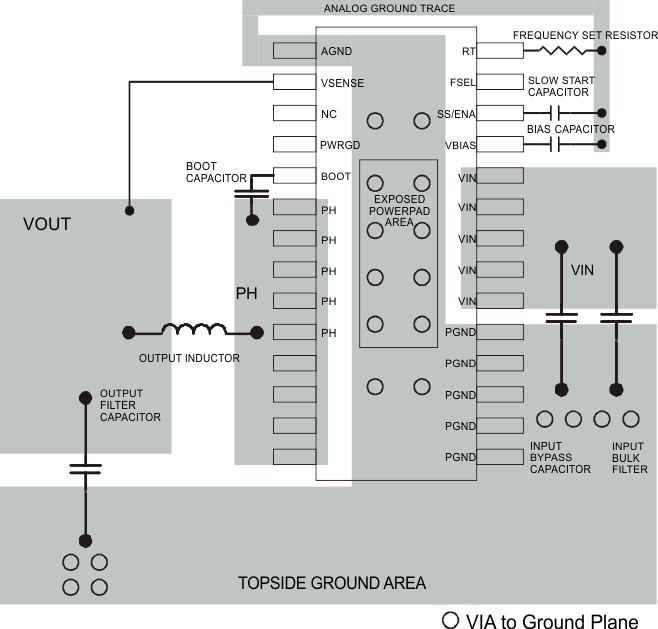 Figure 18. TPS5461x PCB Layout
10.3 Thermal Considerations
For operation at full rated load current, the analog ground plane must provide adequate heat dissipating area. A 3 inch by 3 inch plane of 1 ounce copper is recommended, though not mandatory, depending on ambient temperature and airflow. Most applications have larger areas of internal ground plane available, and the PowerPAD should be connected to the largest area available. Additional areas on the top or bottom layers also help dissipate heat, and any area available should be used when 3 A or greater operation is desired. Connection from the exposes area of the PowerPAD to the analog ground plane layer should be made using 0.013 inch diameter vias to avoid solder wicking through the vias. Eight vias should be in the PowerPAD area with four additional vias located under the device package. The size of the vias under the package, but not in the exposed thermal pad area, can be increased to 0.018. Additional vias beyond the ten recommended that enhance thermal performance should be included in areas not under the device package.
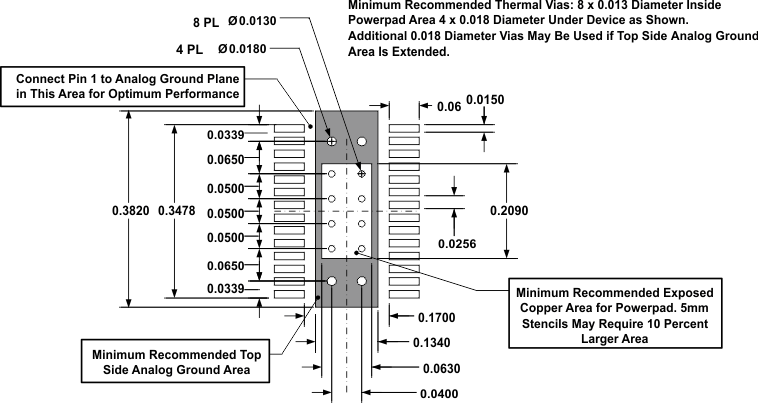 Figure 19. Recommended Land Pattern for 28-Pin PWP PowerPAD 12