SLUSCE4A January 2017 – July 2017 TPS548B22
PRODUCTION DATA.
- 1 Features
- 2 Applications
- 3 Description
- 4 Revision History
- 5 Pin Configuration and Functions
- 6 Specifications
-
7 Detailed Description
- 7.1 Overview
- 7.2 Functional Block Diagram
- 7.3 Feature Description
- 7.4 Device Functional Modes
- 7.5 Programming
-
8 Applications and Implementation
- 8.1 Application Information
- 8.2
Typical Applications
- 8.2.1 TPS548B22 1.5-V to 18-V Input, 1-V Output, 25-A Converter
- 8.2.2 Design Requirements
- 8.2.3
Design Procedure
- 8.2.3.1 Switching Frequency Selection
- 8.2.3.2 Inductor Selection
- 8.2.3.3 Output Capacitor Selection
- 8.2.3.4 Input Capacitor Selection
- 8.2.3.5 Bootstrap Capacitor Selection
- 8.2.3.6 BP Pin
- 8.2.3.7 R-C Snubber and VIN Pin High-Frequency Bypass
- 8.2.3.8 Optimize Reference Voltage (VSEL)
- 8.2.3.9 MODE Pin Selection
- 8.2.3.10 Overcurrent Limit Design.
- 8.2.4 Application Curves
- 9 Power Supply Recommendations
- 10Layout
- 11Device and Documentation Support
- 12Mechanical, Packaging, and Orderable Information
Package Options
Refer to the PDF data sheet for device specific package drawings
Mechanical Data (Package|Pins)
- RVF|40
Thermal pad, mechanical data (Package|Pins)
- RVF|40
Orderable Information
10 Layout
10.1 Layout Guidelines
Consider these layout guidelines before starting a layout work using TPS548B22.
- It is absolutely critical that all GND pins, including AGND (pin 30), DRGND (pin 29), and PGND (pins 13, 14, 15, 16, 17, 18, 19, and 20) are connected directly to the thermal pad underneath the device via traces or plane.
- Include as many thermal vias as possible to support a 25-A thermal operation. For example, a total of 35 thermal vias are used (outer diameter of 20 mil) in the TPS548B22EVM-847 available for purchase at ti.com. (SLUUBE4)
- Place the power components (including input/output capacitors, output inductor and TPS548B22 device) on one side of the PCB (solder side). Insert at least two inner layers (or planes) connected to the power ground, in order to shield and isolate the small signal traces from noisy power lines.
- Place the VIN pin decoupling capacitors as close as possible to the PVIN and PGND pins to minimize the input AC current loop. Place a high-frequency decoupling capacitor (with a value between 1 nF and 0.1 µF) as close to the PVIN pin and PGND pin as the spacing rule allows. This placement helps surpress the switch node ringing.
- Place VDD and BP decoupling capacitors as close as possible to the device pins. Do not use PVIN plane connection for the VDD pin. Separate the VDD signal from the PVIN signal by using separate trace connections. Provide GND vias for each decoupling capacitor and make the loop as small as possible.
- Ensure that the PCB trace defined as switch node (which connects the SW pins and up-stream of the output inductor) are as short and wide as possible. In the TPS548B22EVM-847 design, the SW trace width is 200 mil. Use a separate via or trace to connect SW node to snubber and bootstrap capacitor. Do not combine these connections.
- Place all sensitive analog traces and components (including VOSNS, RSP, RSN, ILIM, MODE, VSEL and FSEL) far away from any high voltage switch node (itself and others), such as SW and BOOT to avoid noise coupling. In addition, place MODE, VSEL and FSEL programming resistors near the device pins.
- The RSP and RSN pins operate as inputs to a differential remote sense amplifier that operates with very high impedance. It is essential to route the RSP and RSN pins as a pair of diff-traces in Kelvin-sense fashion. Route them directly to either the load sense points (+ and –) or the output bulk capacitors. The internal circuit uses the VOSNS pin for on-time adjustment. It is critical to tie the VOSNS pin directly tied to VOUT (load sense point) for accurate output voltage result.
- Pins 6, 7, and 26 are not connected in the 25-A TPS548B22, while pins 6 and 7 connect to SW and pin 26 connects to PVIN in the 40-A TPS548D22.
10.2 Layout Example
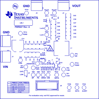 Figure 27. EVM Top View
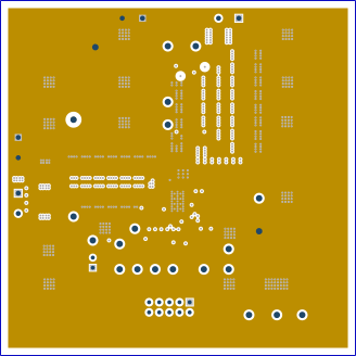 Figure 29. EVM Inner Layer 1
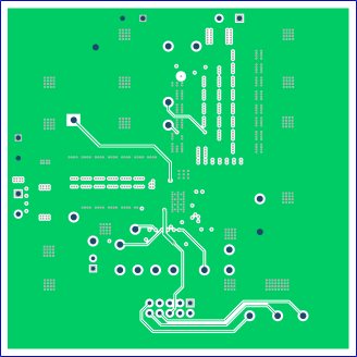 Figure 31. EVM Inner Layer 3
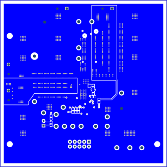 Figure 33. EVM Bottom Layer
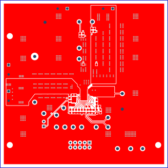 Figure 28. EVM Top Layer
 Figure 30. EVM Inner Layer 2
 Figure 32. EVM Inner Layer 4
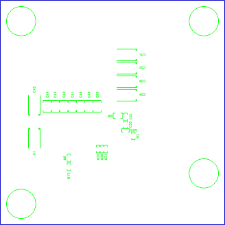 Figure 34. EVM Bottom Symbols
10.2.1 Mounting and Thermal Profile Recommendation
Proper mounting technique adequately covers the exposed thermal tab with solder. Excessive heat during the reflow process can affect electrical performance. Figure 35 shows the recommended reflow oven thermal profile. Proper post-assembly cleaning is also critical to device performance. See TI Application Report QFN/SON PCB Attachment for more information.
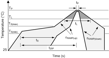 Figure 35. Recommended Reflow Oven Thermal Profile
Table 9. Recommended Thermal Profile Parameters
| PARAMETER | MIN | TYP | MAX | UNIT | |
|---|---|---|---|---|---|
| RAMP UP AND RAMP DOWN | |||||
| rRAMP(up) | Average ramp-up rate, TS(max) to TP | 3 | °C/s | ||
| rRAMP(down) | Average ramp-down rate, TP to TS(max) | 6 | °C/s | ||
| PRE-HEAT | |||||
| TS | Pre-heat temperature | 150 | 200 | °C | |
| tS | Pre-heat time, TS(min) to TS(max) | 60 | 180 | s | |
| REFLOW | |||||
| TL | Liquidus temperature | 217 | °C | ||
| TP | Peak temperature | 260 | °C | ||
| tL | Time maintained above liquidus temperature, TL | 60 | 150 | s | |
| tP | Time maintained within 5 °C of peak temperature, TP | 20 | 40 | s | |
| t25P | Total time from 25 °C to peak temperature, TP | 480 | s | ||