SLUSCE4A January 2017 – July 2017 TPS548B22
PRODUCTION DATA.
- 1 Features
- 2 Applications
- 3 Description
- 4 Revision History
- 5 Pin Configuration and Functions
- 6 Specifications
-
7 Detailed Description
- 7.1 Overview
- 7.2 Functional Block Diagram
- 7.3 Feature Description
- 7.4 Device Functional Modes
- 7.5 Programming
-
8 Applications and Implementation
- 8.1 Application Information
- 8.2
Typical Applications
- 8.2.1 TPS548B22 1.5-V to 18-V Input, 1-V Output, 25-A Converter
- 8.2.2 Design Requirements
- 8.2.3
Design Procedure
- 8.2.3.1 Switching Frequency Selection
- 8.2.3.2 Inductor Selection
- 8.2.3.3 Output Capacitor Selection
- 8.2.3.4 Input Capacitor Selection
- 8.2.3.5 Bootstrap Capacitor Selection
- 8.2.3.6 BP Pin
- 8.2.3.7 R-C Snubber and VIN Pin High-Frequency Bypass
- 8.2.3.8 Optimize Reference Voltage (VSEL)
- 8.2.3.9 MODE Pin Selection
- 8.2.3.10 Overcurrent Limit Design.
- 8.2.4 Application Curves
- 9 Power Supply Recommendations
- 10Layout
- 11Device and Documentation Support
- 12Mechanical, Packaging, and Orderable Information
Package Options
Refer to the PDF data sheet for device specific package drawings
Mechanical Data (Package|Pins)
- RVF|40
Thermal pad, mechanical data (Package|Pins)
- RVF|40
Orderable Information
8 Applications and Implementation
NOTE
Information in the following applications sections is not part of the TI component specification, and TI does not warrant its accuracy or completeness. TI’s customers are responsible for determining suitability of components for their purposes. Customers should validate and test their design implementation to confirm system functionality.
8.1 Application Information
The TPS548B22 device is a highly integrated synchronous step-down DC-DC converters. These devices are used to convert a higher DC input voltage to a lower DC output voltage, with a maximum output current of 25 A. Use the following design procedure to select key component values for this family of devices.
8.2 Typical Applications
8.2.1 TPS548B22 1.5-V to 18-V Input, 1-V Output, 25-A Converter
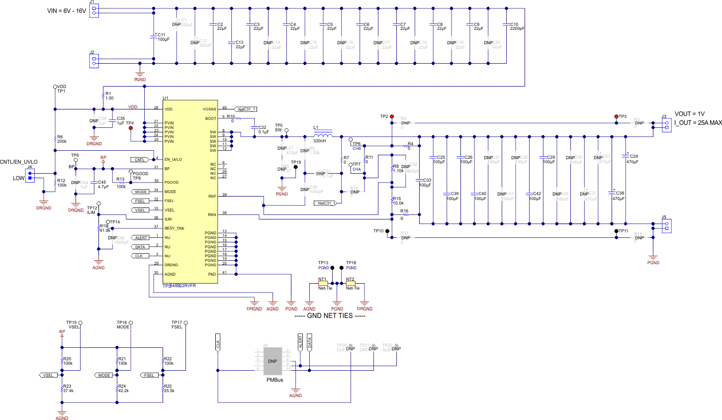 Figure 21. Typical Application Schematic
8.2.2 Design Requirements
For this design example, use the input parameters shown in Table 5.
Table 5. Design Example Specifications
| PARAMETER | TEST CONDITION | MIN | TYP | MAX | UNIT | |
|---|---|---|---|---|---|---|
| VIN | Input voltage | 5 | 12 | 18 | V | |
| VIN(ripple) | Input ripple voltage | IOUT = 25 A | 0.4 | V | ||
| VOUT | Output voltage | 1 | V | |||
| Line regulation | 5 V ≤ VIN ≤ 18 V | 0.5% | ||||
| Load regulation | 0 V ≤ IOUT ≤ 25 A | 0.5% | ||||
| VPP | Output ripple voltage | IOUT = 25 A | 10 | mV | ||
| VOVER | Transient response overshoot | ISTEP = 15 A | 30 | mV | ||
| VUNDER | Transient response undershoot | ISTEP = 15 A | 30 | mV | ||
| IOUT | Output current | 5 V ≤ VIN ≤ 18 V | 25 | A | ||
| tSS | Soft-start time | 1 | ms | |||
| IOC | Overcurrent trip point(1) | 32 | A | |||
| η | Peak efficiency | IOUT = 7 A | 90% | |||
| fSW | Switching frequency | 650 | kHz | |||
8.2.3 Design Procedure
8.2.3.1 Switching Frequency Selection
Select a switching frequency for the regulator. There is a trade off between higher and lower switching frequencies. Higher switching frequencies may produce smaller a solution size using lower valued inductors and smaller output capacitors compared to a power supply that switches at a lower frequency. However, the higher switching frequency causes extra switching losses, which decrease efficiency and impact thermal performance. In this design, a moderate switching frequency of 650 kHz achieves both a small solution size and a high-efficiency operation with the frequency selected.
Select one of four switching frequencies and FSEL resistor values from Table 6. The recommended high-side RFSEL value is 100 kΩ (1%). Choose a low-side resistor value from Table 6 based on the choice of switching frequency. For each switching frequency selection, there are multiple values of RFSEL(LS) to choose from. In order to select the correct value, additional considerations (internal ramp compensation and light load operation) other than switching frequency need to be included.
Table 6. FSEL Pin Selection
| SWITCHING FREQUENCY fSW (kHz) |
FSEL VOLTAGE VFSEL (V) |
HIGH-SIDE RESISTOR RFSEL(HS) (kΩ) 1% or better |
LOW-SIDE RESISTOR RFSEL(LS) (kΩ) 1% or better |
|
|---|---|---|---|---|
| MAXIMUM | MINIMUM | |||
| 1050 | 2.93 | 1.465 | 100 | Open |
| 187 | ||||
| 165 | ||||
| 147 | ||||
| 133 | ||||
| 121 | ||||
| 110 | ||||
| 100 | ||||
| 875 | 1.396 | 0.869 | 100 | 90.9 |
| 82.5 | ||||
| 75 | ||||
| 68.1 | ||||
| 60.4 | ||||
| 53.6 | ||||
| 47.5 | ||||
| 42.2 | ||||
| 650 | 0.798 | 0.366 | 100 | 37.4 |
| 33.2 | ||||
| 29.4 | ||||
| 25.5 | ||||
| 22.1 | ||||
| 19.1 | ||||
| 16.5 | ||||
| 14.3 | ||||
| 425 | 0.317 | 0 | 100 | 12.1 |
| 10 | ||||
| 7.87 | ||||
| 6.19 | ||||
| 4.64 | ||||
| 3.16 | ||||
| 1.78 | ||||
| 0 | ||||
There is some limited freedom to choose FSEL resistors that have other than the recommended values. The criteria is to ensure that for particular selection of switching frequency, the FSEL voltage is within the maximum and minimum FSEL voltage levels listed in Table 6. Use Equation 2 to calculate the FSEL voltage. Select FSEL resistors that include tolerances of 1% or better.

where
- VBP(det) is the voltage used by the device to program the level of valid FSEL pin voltage during initial device start-up (2.9 V typical)
In addition to serving the frequency select purpose, the FSEL pin can also be used to program internal ramp compensation (DCAP3) and light-load conduction mode. When DCAP3 mode is selected (see section 8.2.3.9), internal ramp compensation is used for stabilizing the converter design. The internal ramp compensation is a function of the switching frequency (fSW) and the duty cycle range (the output voltage-to-input voltage ratio). Table 7 summarizes the ramp choices using these functions.
Table 7. Switching Frequency Selection
| SWITCHING FREQUENCY SETTING (fSW) (kHz) |
RAMP SELECT OPTION |
TIME CONSTANT t (µs) |
VOUT RANGE (FIXED VIN = 12 V) |
DUTY CYCLE RANGE (VOUT/VIN) (%) |
||
| MIN | MAX | MIN | MAX | |||
| 425 | R/2 | 9 | 0.6 | 0.9 | 5 | 7.5 |
| R × 1 | 16.8 | 0.9 | 1.5 | 7.5 | 12.5 | |
| R × 2 | 32.3 | 1.5 | 2.5 | 12.5 | 21 | |
| R × 3 | 55.6 | 2.5 | 5.5 | >21 | ||
| 650 | R/2 | 7 | 0.6 | 0.9 | 5 | 7.5 |
| R × 1 | 13.5 | 0.9 | 1.5 | 7.5 | 12.5 | |
| R × 2 | 25.9 | 1.5 | 2.5 | 12.5 | 21 | |
| R × 3 | 44.5 | 2.5 | 5.5 | >21 | ||
| 875 | R/2 | 5.6 | 0.6 | 0.9 | 5 | 7.5 |
| R × 1 | 10.4 | 0.9 | 1.5 | 7.5 | 12.5 | |
| R × 2 | 20 | 1.5 | 2.5 | 12.5 | 21 | |
| R × 3 | 34.4 | 2.5 | 5.5 | >21 | ||
| 1050 | R/2 | 3.8 | 0.6 | 0.9 | 5 | 7.5 |
| R × 1 | 7.1 | 0.9 | 1.5 | 7.5 | 12.5 | |
| R × 2 | 13.6 | 1.5 | 2.5 | 12.5 | 21 | |
| R × 3 | 23.3 | 2.5 | 5.5 | >21 | ||
The FSEL pin programs the light-load selection. TPS548B22 device supports either SKIP mode or FCCM operations. For optimized light-load efficiency, it is recommended to program the device to operate in SKIP mode. For better load regulation from no load to full load, it is recommended to program the device to operate in FCCM mode.
RFSEL(LS) can be determined after determining the switching frequency, ramp and light-load operation. Table 2 lists the full range of choices.
8.2.3.2 Inductor Selection
To calculate the value of the output inductor, use Equation 3. The coefficient KIND represents the amount of inductor ripple current relative to the maximum output current. The output capacitor filters the inductor ripple current. Therefore, choosing a high inductor ripple current impacts the selection of the output capacitor since the output capacitor must have a ripple current rating equal to or greater than the inductor ripple current. In general, maintain a KIND coefficient greater than 0 and 0.4 for balanced performance. Using this target ripple current, the required inductor size can be calculated as shown in Equation 3:

Selecting a KIND of 0.2, the target inductance L1 = 290 nH. Using the next standard value, the 330 nH is chosen in this application for its high current rating, low DCR, and small size. The inductor ripple current, RMS current, and peak current can be calculated using Equation 4, Equation 5 and Equation 6. These values should be used to select an inductor with approximately the target inductance value, and current ratings that allow normal operation with some margin.


8.2.3.3 Output Capacitor Selection
There are three primary considerations for selecting the value of the output capacitor. The output capacitor affects three criteria:
- Stability
- Regulator response to a change in load current or load transient
- Output voltage ripple
These three considerations are important when designing regulators that must operate where the electrical conditions are unpredictable. The output capacitance needs to be selected based on the most stringent of these three criteria.
8.2.3.3.1 Minimum Output Capacitance to Ensure Stability
To prevent sub-harmonic multiple pulsing behavior, TPS548B22 application designs must strictly follow the small signal stability considerations described in Equation 7.

where
- COUT(min) is the minimum output capacitance needed to meet the stability requirement of the design
- tON is the on-time information based on the switching frequency and duty cycle (in this design, 128 ns)
- τ is the ramp compensation time constant of the design based on the switching frequency and duty cycle, (in this design, 25.9 µs, refer to Table 7)
- LOUT is the output inductance (in the design, 0.33 µH)
- VREF is the user-selected reference voltage level (in this design, 1 V)
- VOUT is the output voltage (in this design, 1 V)
The minimum output capacitance calculated from Equation 7 is 40 µF. The stability is ensured when the amount of the output capacitance is 40 µF or greater. And when all MLCCs (multi-layer ceramic capacitors) are used, both DC and AC derating effects must be considered to ensure that the minimum output capacitance requirement is met with sufficient margin.
8.2.3.3.2 Response to a Load Transient
The output capacitance must supply the load with the required current when current is not immediately provided by the regulator. When the output capacitor supplies load current, the impedance of the capacitor greatly affects the magnitude of voltage deviation (such as undershoot and overshoot) during the transient.
Use Equation 8 and Equation 9 to estimate the amount of capacitance needed for a given dynamic load step and release.
NOTE
There are other factors that can impact the amount of output capacitance for a specific design, such as ripple and stability.


where
- COUT(min_under) is the minimum output capacitance to meet the undershoot requirement
- COUT(min_over)is the minimum output capacitance to meet the overshoot requirement
- L is the output inductance value (0.33 µH)
- ∆ILOAD(max) is the maximum transient step (15 A)
- VOUT is the output voltage value (1 V)
- tSW is the switching period (1.54 µs)
- VIN(min) is the minimum input voltage for the design (10.8 V)
- tOFF(min) is the minimum off time of the device (300 ns)
- ∆VLOAD(insert) is the undershoot requirement (30 mV)
- ∆VLOAD(release) is the overshoot requirement (30 mV)
Most of the above parameters can be found in Table 5.
The minimum output capacitance to meet the undershoot requirement is 516 µF. The minimum output capacitance to meet the overshoot requirement is 1238 µF. This example uses a combination of POSCAP and MLCC capacitors to meet the overshoot requirement.
- POSCAP bank no. 1: 2 × 470 µF, 2.5 V, 6 mΩ per capacitor
- MLCC bank no. 2: 7 × 100 µF, 6.3 V, 2 mΩ per capacitor with DC+AC derating factor of 60%
Recalculating the worst case overshoot using the described capacitor bank design, the overshoot is 29 mV, which meets the 30-mV overshoot specification requirement.
8.2.3.3.3 Output Voltage Ripple
The output voltage ripple is another important design consideration. Equation 10 calculates the minimum output capacitance required to meet the output voltage ripple specification. This criterion is the requirement when the impedance of the output capacitance is dominated by ESR.

In this case, the maximum output voltage ripple is 10 mV. For this requirement, the minimum capacitance for ripple requirement yields 82 µF. Because this capacitance value is significantly lower compared to that of transient requirement, determine the capacitance bank from Response to a Load Transient. Because the output capacitor bank consists of both POSCAP and MLCC type capacitors, it is important to consider the ripple effect at the switching frequency due to effective ESR. Use Equation 11 to determine the maximum ESR of the output capacitor bank for the switching frequency.

Estimate the effective ESR at the switching frequency by obtaining the impedance vs frequency characteristics of the output capacitors. The parallel impedance of capacitor bank #1 and capacitor bank #2 at the switching frequency of the design example is estimated to be 1.2 mΩ, which is less than that of the maximum ESR value. Therefore, the output voltage ripple requirement (10 mV) can be met. For detailed calculation on the effective ESR please contact the factory to obtain a user-friendly Excel based design tool.
8.2.3.4 Input Capacitor Selection
The TPS548B22 requires a high-quality, ceramic, type X5R or X7R, input decoupling capacitor with a value of at least 1 μF of effective capacitance on the VDD pin, relative to AGND. The power stage input decoupling capacitance (effective capacitance at the PVIN and PGND pins) must be sufficient to supply the high switching currents demanded when the high-side MOSFET switches on, while providing minimal input voltage ripple as a result. This effective capacitance includes any DC bias effects. The voltage rating of the input capacitor must be greater than the maximum input voltage. The capacitor must also have a ripple current rating greater than the maximum input current ripple to the device during full load. The input ripple current can be calculated using Equation 12.

The minimum input capacitance and ESR values for a given input voltage ripple specification, VIN(ripple), are shown in Equation 13 and Equation 14. The input ripple is composed of a capacitive portion, VRIPPLE(cap), and a resistive portion, VRIPPLE(esr).


The value of a ceramic capacitor varies significantly over temperature and the amount of DC bias applied to the capacitor. The capacitance variations due to temperature can be minimized by selecting a dielectric material that is stable over temperature. X5R and X7R ceramic dielectrics are usually selected for power regulator capacitors because they have a high capacitance to volume ratio and are fairly stable over temperature. The input capacitor must also be selected with the DC bias taken into account. For this example design, a ceramic capacitor with at least a 25-V voltage rating is required to support the maximum input voltage. For this design, allow 0.1-V input ripple for VRIPPLE(cap), and 0.1-V input ripple for VRIPPLE(esr). Using Equation 13 and Equation 14, the minimum input capacitance for this design is 21.4 µF, and the maximum ESR is 3.4 mΩ. For this example, four 22-μF, 25-V ceramic capacitors and one additional 100-μF, 25-V low-ESR polymer capacitors in parallel were selected for the power stage.
8.2.3.5 Bootstrap Capacitor Selection
A ceramic capacitor with a value of 0.1 μF must be connected between the BOOT and SW pins for proper operation. It is recommended to use a ceramic capacitor with X5R or better grade dielectric. Use a capacitor with a voltage rating of 25 V or higher.
8.2.3.6 BP Pin
Bypass the BP pin to DRGND with 4.7-µF capacitance. In order for the regulator to function properly, it is important that these capacitors be localized to the , with low-impedance return paths. See Layout Guidelines section for more information.
8.2.3.7 R-C Snubber and VIN Pin High-Frequency Bypass
Though it is possible to operate the TPS548B22 within absolute maximum ratings without ringing reduction techniques, some designs may require external components to further reduce ringing levels. This example uses two approaches: a high frequency power stage bypass capacitor on the VIN pins, and an R-C snubber between the SW area and GND.
The high-frequency VIN bypass capacitor is a lossless ringing reduction technique which helps minimizes the outboard parasitic inductances in the power stage, which store energy during the low-side MOSFET on-time, and discharge once the high-side MOSFET is turned on. For this example twoone 2.2-nF, 25-V, 0603-sized high-frequency capacitors are used. The placement of these capacitors is critical to its effectiveness. Its ideal placement is shown in Figure 21.
Additionally, an R-C snubber circuit is added to this example. To balance efficiency and spike levels, a 1-nF capacitor and a 1-Ω resistor are chosen. In this example a 0805-sized resistor is chosen, which is rated for 0.125 W, nearly twice the estimated power dissipation. See SLUP100 for more information about snubber circuits.
8.2.3.8 Optimize Reference Voltage (VSEL)
Optimize the reference voltage by choosing a value for RVSEL. The TPS548B22 device is designed with a wide range of precision reference voltage support from 0.6 V to 1.2 V with an available step change of 50 mV. Program these reference voltages using the VSEL pin strap configurations. See Table 3 for internal reference voltage selections. In addition to providing initial boot voltage value, use the VSEL pin to program hiccup and latch-off mode.
There are two ways to program the output voltage set point. If the output voltage set point is one of the 16 available reference and boot voltage options, no feedback resistors are required for output voltage programming. In the case where feedback resistors are not needed, connect the RSP pin to the positive sensing point of the load. Always connect the RSN pin to the load return sensing point.
In this design example, since the output voltage set point is 1 V, selecting RVSEL(LS) of either 75 kΩ (latch off) or 68.1 kΩ (hiccup). If the output voltage set point is NOT one of the 16 available reference or boot voltage options, feedback resistors are required for output voltage programming. Connect the RSP pin to the mid-point of the resistor divider. Always connect the RSN pin to the load return sensing point as shown in Figure 19 and Figure 20.
The general guideline to select boot and internal reference voltage is to select the reference voltage closest to the output voltage set point. In addition, because the RSP and RSN pins are extremely high-impedance input terminals of the true differential remote sense amplifier, use a feedback resistor divider with values much less than 100 kΩ.
8.2.3.9 MODE Pin Selection
MODE pin strap configuration is used to program control topology and internal soft-start timing selections. TPS548B22 supports both DCAP3 and DCAP operation. For general POL applications, it is strongly recommended to configure the control topology to be DCAP3 due to its simple to use and no external compensation features. In the rare instance where DCAP is needed, an RCC network across the output inductor is needed to generate sufficient ripple voltage on the RSP pin. In this design example, RMODE(LS) of 22.1 kΩ is selected for DCAP3 and soft start time of 1 ms.
8.2.3.10 Overcurrent Limit Design.
The TPS548B22 device uses the ILIM pin to set the OCP level. Connect the ILIM pin to GND through the voltage setting resistor, RILIM. In order to provide both good accuracy and cost effective solution, this device supports temperature compensated MOSFET on-resistance (RDS(on)) sensing. Also, this device performs both positive and negative inductor current limiting with the same magnitudes. Positive current limit is normally used to protect the inductor from saturation therefore causing damage to the high-side and low-side FETs. Negative current limit is used to protect the low-side FET during OVP discharge.
The inductor current is monitored by the voltage between PGND pin and SW pin during the OFF time. The ILIM pin has 1200 ppm/°C temperature slope to compensate the temperature dependency of the on-resistance. The PGND pin is used as the positive current sensing node.
TPS548B22 has cycle-by-cycle over-current limiting control. The inductor current is monitored during the OFF state and the controller maintains the OFF state during the period that the inductor current is larger than the overcurrent ILIM level. The voltage on the ILIM pin (VILIM) sets the valley level of the inductor current. The range of value of the RILIM resistor is between 9.53 kΩ and 105 kΩ. The range of valley OCL is between 5 A and 50 A (typical). If the RILIM resistance is outside of the recommended range, OCL accuracy and function cannot be assured. (see Table 8)
Table 8. OCP Valley Settings
| 1% RILIM
(kΩ) |
OVERCURRENT PROTECTION VALLEY (A) |
| 82.1 | 40 |
| 71.5 | 35 |
| 61.9 | 30 |
| 51.1 | 25 |
| 40.2 | 20 |
| 30.1 | 15 |
| 20.5 | 10 |
Use Equation 15 to relate the valley OCL to the RILIM resistance.
where
- RILIM is in kΩ
- OCLVALLEY is in A
In this design example, the desired valley OCL is 30 A, the calculated RILIM is 61.9 kΩ. Use Equation 16 to calculate the DC OCL to be 32.1 A.

where
- RILIM is in kΩ
- OCLDC is in A
In an overcurrent condition, the current to the load exceeds the inductor current and the output voltage falls. When the output voltage crosses the under-voltage fault threshold for at least 1msec, the behavior of the device depends on the VSEL pin strap setting. If hiccup mode is selected, the device will restart after 16-ms delay (1-ms soft-start option). If the overcurrent condition persists, the OC hiccup behavior repeats. During latch-off mode operation the device shuts down until the EN pin is toggled or VDD pin is power cycled.
8.2.4 Application Curves
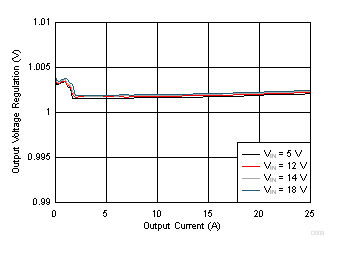
| VDD = VIN | fSW = 650 kHz | SKIP Mode |
| VOUT = 1 V |
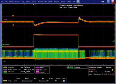
| VDD = VIN = 12 V | fSW = 650 kHz | SKIP Mode |
| VOUT = 1 V | 0.5 A DC with 15-A step at 40A/µs | |
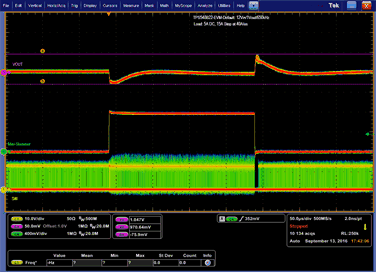
| VDD = VIN = 12 V | fSW = 650 kHz | FCCM Mode | ||
| VOUT = 1 V | 5 A DC with 15-A step at 40A/µs | |||
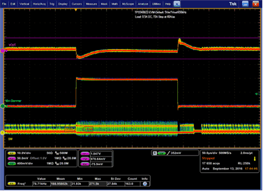
| VDD = VIN = 5 V | fSW = 650 kHz | SKIP Mode |
| VOUT = 1 V | 0.5 A DC with 15-A step at 40A/µs | |
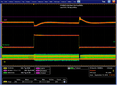
| VDD = VIN = 5 V | fSW = 650 kHz | FCCM Mode |
| VOUT = 1 V | 5 A DC with 15-A step at 40A/µs | |