SNVSB02C March 2020 – July 2021 TPS54JA20
PRODUCTION DATA
- 1 Features
- 2 Applications
- 3 Description
- 4 Revision History
- 5 Pin Configuration and Functions
- 6 Specifications
-
7 Detailed Description
- 7.1 Overview
- 7.2 Functional Block Diagram
- 7.3
Feature Description
- 7.3.1 Internal VCC LDO And Using External Bias On VCC Pin
- 7.3.2 Enable
- 7.3.3 Output Voltage Setting
- 7.3.4 Internal Fixed Soft Start and External Adjustable Soft Start
- 7.3.5 External REFIN For Output Voltage Tracking
- 7.3.6 Frequency and Operation Mode Selection
- 7.3.7 D-CAP3 Control
- 7.3.8 Low-side FET Zero-Crossing
- 7.3.9 Current Sense and Positive Overcurrent Protection
- 7.3.10 Low-side FET Negative Current Limit
- 7.3.11 Power Good
- 7.3.12 Overvoltage and Undervoltage Protection
- 7.3.13 Out-Of-Bounds (OOB) Operation
- 7.3.14 Output Voltage Discharge
- 7.3.15 UVLO Protection
- 7.3.16 Thermal Shutdown
- 7.4 Device Functional Modes
-
8 Application and Implementation
- 8.1 Application Information
- 8.2
Typical Application
- 8.2.1 Design Requirements
- 8.2.2
Detailed Design Procedure
- 8.2.2.1 Output Voltage Setting Point
- 8.2.2.2 Choose the Switching Frequency and the Operation Mode
- 8.2.2.3 Choose the Inductor
- 8.2.2.4 Set the Current Limit (TRIP)
- 8.2.2.5 Choose the Output Capacitor
- 8.2.2.6 Choose the Input Capacitors (CIN)
- 8.2.2.7 Soft Start Capacitor (SS/REFIN Pin)
- 8.2.2.8 EN Pin Resistor Divider
- 8.2.2.9 VCC Bypass Capacitor
- 8.2.2.10 BOOT Capacitor
- 8.2.2.11 PGOOD Pullup Resistor
- 8.2.3 Application Curves
- 9 Power Supply Recommendations
- 10Layout
- 11Device and Documentation Support
- 12Mechanical, Packaging, and Orderable Information
Package Options
Mechanical Data (Package|Pins)
- RWW|21
Thermal pad, mechanical data (Package|Pins)
Orderable Information
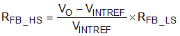
7.3.3 Output Voltage Setting
The output voltage is programmed by the voltage divider resistors, RFB_HS and RFB_LS. Connect RFB_HS between the FB pin and the positive node of the load, and connect RFB_LS between the FB pin and VSNS– pin. The recommended RFB_LS value is 10 kΩ, ranging from 1 kΩ to 20 kΩ. Determine RFB_HS by using Equation 1.
The FB accuracy is determined by two elements. The first element is the accuracy of the internal 900-mV reference, which will be applied to the SS/REFIN pin unless an external VREF is applied. The TPS54JA20 device offers ±0.5% VINTREF accuracy from 0°C to 85°C, and ±1.0% VINTREF accuracy from -40°C to 125°C. The second element is the SS/REFIN-to-FB accuracy, which tells you how accurately the control loop regulates FB node to SS/REFIN pin. The TPS54JA20 device offers ±0.6% SS/REFIN-to-FB accuracy from -40°C to 125°C. For example, when operating from 0°C to 85°C, the total FB accuracy is ±1.1% which includes the impact from chip junction temperature and also the variation from part to part.
To improve the overall VOUT accuracy, using ±1% accuracy or better resistor for the FB voltage divider is highly recommended.
Regardless of remote sensing or single-end sensing connection, the FB voltage divider, RFB_HS and RFB_LS, should be always placed as close as possible to the device.