SLVSAV0B April 2011 – October 2014 TPS55010
PRODUCTION DATA.
- 1 Features
- 2 Applications
- 3 Description
- 4 Simplified Schematic
- 5 Revision History
- 6 Pin Configuration and Functions
- 7 Specifications
-
8 Detailed Description
- 8.1 Overview
- 8.2 Functional Block Diagram
- 8.3
Feature Description
- 8.3.1 Fixed Frequency PWM Control
- 8.3.2 Half Bridge and Bootstrap Voltage
- 8.3.3 Error Amplifier
- 8.3.4 Voltage Reference
- 8.3.5 Adjusting the Output Voltage
- 8.3.6 Enable and Adjusting Undervoltage Lockout
- 8.3.7 Adjusting Slow Start Time
- 8.3.8 Constant Switching Frequency and Timing Resistor (RT/CLK Pin)
- 8.3.9 How to Interface to RT/CLK Pin
- 8.3.10 Overcurrent Protection
- 8.3.11 Reverse Overcurrent Protection
- 8.3.12 FAULT Pin
- 8.3.13 Thermal Shutdown
- 8.4 Device Functional Modes
-
9 Application And Implementation
- 9.1 Application Information
- 9.2
Typical Applications
- 9.2.1 Design Guide - Step-by-Step Design Procedure
- 9.2.2 Primary Side Voltage
- 9.2.3 Voltage Feedback
- 9.2.4 Selecting the Switching Frequency and Primary Inductance
- 9.2.5 Primary Side Capacitor
- 9.2.6 Secondary Side Diode
- 9.2.7 Secondary Side Capacitor
- 9.2.8 Input Capacitor
- 9.2.9 Y - Capacitor
- 9.2.10 Slow Start Capacitor
- 9.2.11 Bootstrap Capacitor Selection
- 9.2.12 UVLO Resistors
- 9.2.13 Compensation
- 9.2.14 Design Tips
- 9.2.15 How to Specify a Fly-Buck Transformer
- 9.2.16 Application Curves
- 9.3 Typical Application, Dual Output
- 10Power Supply Recommendations
- 11Layout
- 12Device and Documentation Support
- 13Mechanical, Packaging, and Orderable Information
Package Options
Mechanical Data (Package|Pins)
- RTE|16
Thermal pad, mechanical data (Package|Pins)
- RTE|16
Orderable Information
8 Detailed Description
8.1 Overview
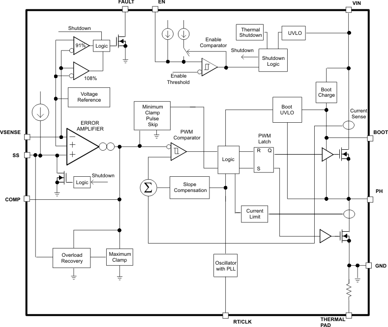
The TPS55010 is a half bridge transformer driver designed to implement a high efficiency, low power isolated supply. The primary side feedback implemented using two resistors and a primary side capacitor provides excellent regulation over line and load compared to an open loop push pull converter.
The half bridge power stage consists of two integrated n-channel MOSFETs with 45 mΩ on resistance. The drive voltage for the integrated high side MOSFET is supplied by a capacitor between the BOOT and PH pins. The switching frequency is adjusted using a resistor to ground on the RT/CLK pin. The device has an internal phase lock loop (PLL) on the RT/CLK pin that is used to synchronize the high side power switch turn on to a falling edge of an external system clock. The wide switching frequency of 100 kHz to 2000 kHz (300kHz to 2000kHz in CLK mode) allows for efficiency, size optimization or noise avoidance when selecting the switching frequency. The TPS55010 has a typical default start up voltage of 2.6 V. The EN pin has an internal pull-up current source that can be used to adjust the input voltage under voltage lockout (UVLO) with two external resistors. In addition, the pull up current provides a default condition when the EN pin is floating for the device to operate. The total operating current for the TPS55010 is typically 360 µA when not switching and under no load. When the device is disabled, the supply current is less than 5 µA. The slow start (SS) pin is used to minimize inrush currents during start up.
8.2 Functional Block Diagram
8.3 Feature Description
8.3.1 Fixed Frequency PWM Control
The TPS55010 uses an adjustable fixed frequency, peak current mode control. The primary voltage is compared through external resistors on the VSENSE pin to an internal voltage reference by an error amplifier which drives the COMP pin. An internal oscillator initiates the turn on of the high side power switch. The error amplifier output is compared to the high side power switch current. When the power switch current reaches the COMP voltage level the high side power switch is turned off and the low side power switch is turned on. The COMP pin voltage increases and decreases as the output current increases and decreases. The device implements a current limit by clamping the COMP pin voltage to a maximum level. The TPS55010 adds a compensating ramp to the switch current signal. This slope compensation prevents sub-harmonic oscillations as duty cycle increases.
8.3.2 Half Bridge and Bootstrap Voltage
The TPS55010 has an integrated boot regulator and requires a small ceramic capacitor between the BOOT and PH pin to provide the gate drive voltage for the high side MOSFET. The value of the ceramic capacitor should be 0.1 µF. A ceramic capacitor with an X7R or X5R grade dielectric and a voltage rating of 10 V or higher is recommended because of the stable characteristics over temperature and voltage.
8.3.3 Error Amplifier
The TPS55010 uses a transconductance error amplifier. The amplifier compares the VSENSE voltage to the lower of the SS pin voltage or the internal 0.829 V voltage reference. The transconductance of the error amplifier is 245 µA/V. The frequency compensation components are placed between the COMP pin and ground.
8.3.4 Voltage Reference
The voltage reference system produces a precise ±3.0% voltage reference over temperature by scaling the output of a temperature-stable band gap circuit. The band gap and scaling circuits produce 0.829 V at the non-inverting input of the error amplifier.
8.3.5 Adjusting the Output Voltage
The primary side voltage is set with a resistor divider from the primary side capacitor to the VSENSE pin. It is recommended to use 1% tolerance or better divider resistors. Start with a 10 kΩ for the RLS resistor and use Equation 1 to calculate RHS. The output voltage is a function of the primary voltage, transformer turns ratio and forward voltage of the diode.

spacer

spacer
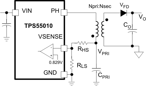 Figure 17. Setting the Output Voltage
8.3.6 Enable and Adjusting Undervoltage Lockout
The TPS55010 is disabled when the VIN pin voltage falls below 2.6 V. If an application requires a higher undervoltage lockout (UVLO), use the EN pin as shown in Figure 18 to adjust the input voltage UVLO by using two external resistors. The EN pin has an internal pull-up current source of 1.2 µA that provides the default condition of the TPS55010 operating when the EN pin floats. Once the EN pin voltage exceeds 1.25 V, an additional 3.4 µA of hysteresis is added. When the EN pin is pulled below 1.18 V, the hysteresis current is removed.
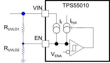 Figure 18. Adjustable Under Voltage Lock Out
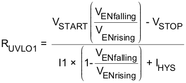
spacer

8.3.7 Adjusting Slow Start Time
A capacitor on the SS pin to ground implements a slow start time to minimize inrush current during startup. The TPS55010 regulates to the lower of the SS pin and the internal reference voltage. The TPS55010 has an internal pull-up current source of 2.2 µA which charges the external slow start capacitor. Equation 5 calculates the required slow start capacitor value where TSS is the desired slow start time in ms, Iss is the internal slow start charging current of 2.2 µA, and VREF is the internal voltage reference of 0.829 V.
If during normal operation, the VIN goes below the UVLO, EN pin pulled below 1.18 V, or a thermal shutdown event occurs, the TPS55010 stops switching. When the VIN goes above UVLO, EN is released or pulled high, or a thermal shutdown is exited, then SS is discharged to below 40 mV before reinitiating a powering up sequence. The VSENSE voltage will follow the SS pin voltage with a 35 mV offset up to 85% of the internal voltage reference. When the SS voltage is greater than 85% on the internal reference voltage the offset increases as the effective system reference transitions from the SS voltage to the internal voltage reference. If no slow start time is needed, the SS pin can be left open. The slow start capacitor should be less than 0.47 µF.

8.3.8 Constant Switching Frequency and Timing Resistor (RT/CLK Pin)
The switching frequency of the TPS55010 is adjustable over a wide range from 100 kHz to 2000 kHz by placing a maximum of 1070 kΩ and minimum of 42.2 kΩ, respectively, on the RT/CLK pin. An internal amplifier holds this pin at a fixed voltage when using an external resistor to ground to set the switching frequency. The RT/CLK is typically 0.5 V. To determine the timing resistance for a given switching frequency, use Equation 6.
To reduce the solution size one would typically set the switching frequency as high as possible, but tradeoffs of the efficiency, maximum input voltage and minimum controllable on time should be considered. The minimum controllable on time is typically 130 ns.

8.3.9 How to Interface to RT/CLK Pin
The RT/CLK pin can be used to synchronize the regulator to an external system clock. To implement the synchronization feature connect a square wave to the RT/CLK pin through one of the circuit networks shown in Figure 19. The square wave amplitude must transition lower than 0.4V and higher than 2.2V on the RT/CLK pin and have a high time greater than 75 ns. The synchronization frequency range is 300 kHz to 2000 kHz. The rising edge of the PH is synchronized to the falling edge of RT/CLK pin signal.
The external synchronization circuit should be designed in such a way that the device has the default frequency set resistor connected from the RT/CLK pin to ground should the synchronization signal turn off. It is recommended to use a frequency set resistor connected as shown in Figure 19 through another resistor (e.g 50 Ω) to ground for clock signal that are not Hi-Z or tri-state during the off state. The RT resistor value should set the switching frequency close to the external CLK frequency. It is recommended to ac couple the synchronization signal through a 10 pF ceramic capacitor to RT/CLK pin. The first time the CLK is pulled above the CLK threshold the device switches from the RT resistor frequency to PLL mode. The internal 0.5 V voltage source is removed and the CLK pin becomes high impedance as the PLL starts to lock onto the external signal. Since there is a PLL on the regulator the switching frequency can be higher or lower than the frequency set with the external resistor. The device transitions from the resistor mode to the PLL mode and then will increase or decrease the switching frequency until the PLL locks onto the external CLK frequency within 50 microseconds. When the device transitions from the PLL to resistor mode the switching frequency will slow down from the CLK frequency to 150 kHz, then reapply the 0.5V voltage and the resistor will then set the switching frequency.
 Figure 19. Synchronizing to a System Clock
8.3.10 Overcurrent Protection
The TPS55010 implements a cycle by cycle current limit. During each switching cycle the high side switch current is compared to the voltage on the COMP pin. When the instantaneous switch current intersects the COMP voltage, the high side switch is turned off. During overcurrent conditions that pull the output voltage low, the error amplifier responds by driving the COMP pin high, increasing the switch current. The error amplifier output is clamped internally. This clamp functions as a switch current limit.
8.3.11 Reverse Overcurrent Protection
The TPS55010 implements low side current protection by detecting the voltage across the low side MOSFET. When the converter sinks current through its low side FET, the control circuit turns off the low side MOSFET if the reverse current is more than 4.5 A
8.3.12 FAULT Pin
The FAULT pin output is an open drain MOSFET. The output is pulled low when the VSENSE voltage is below 91% or rising above 108% of the nominal internal reference voltage. It is recommended to use a pull-up resistor between the values of 1kΩ and 100kΩ to a voltage source that is 6 V or less. The FAULT pin is in a valid state once the VIN input voltage is greater than 1.6 V. The FAULT pin is pulled low, if the input UVLO or thermal shutdown is asserted, or the EN pin is pulled low.
8.3.13 Thermal Shutdown
The device implements an internal thermal shutdown to protect itself if the junction temperature exceeds 171°C. The thermal shutdown forces the device to stop switching when the junction temperature exceeds the thermal trip threshold. Once the die temperature decreases below 159°C, the device reinitiates the power up sequence by discharging the SS pin to below 40 mV. The thermal shutdown hysteresis is 12°C.
8.4 Device Functional Modes
8.4.1 Operation of the Fly-Buck™ Converter
Figure 20 shows a simplified schematic and the two primary operational states of the Fly-Buck converter. The power supply is a variation of a Flyback converter and consists of a half bridge power stage SHS and SLS, transformer, primary side capacitor, diode and output capacitor. The output voltage is regulated indirectly by using the primary side capacitor voltage, VPRI, as feedback. The Fly-Buck is a portmanteau of flyback and buck since the transformer is connected as a flyback converter and the input to output voltage relationship is similar to a buck derived converter, assuming the converter is operating in steady state and the transformer has negligible leakage inductance.
The CPRI and LPRI are charged by the input voltage source VIN during the time the high side switch SHS is on. During this time, diode D1 is reversed biased and the load current is supplied by output capacitor CO.
During the off time of SHS, SLS conducts and the voltage on CPRI continues to increase during a portion of the SLS conduction time. The voltage increase is due to the energy transfer from LPRI to CPRI. For the remaining portion of the SLS conduction time, the CPRI voltage decreases because of current in LPRI reverses; see the ILPRI and VPRI waveforms in Figure 21. By neglecting the diode voltage drop, conduction dead time and leakage inductance, the input to output voltage conversion ratio can be derived as shown in Equation 7 from the flux balance in LPRI. It can be seen in Equation 7 that the input to output relationship is the same as a buck-derived converter with transformer isolation. The dc voltage VPRI on the primary side capacitor in Equation 8 has the same linear relationship to the input voltage as a buck converter.
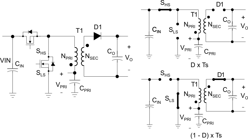 Figure 20. Output Voltage Conversion Ratio

spacer

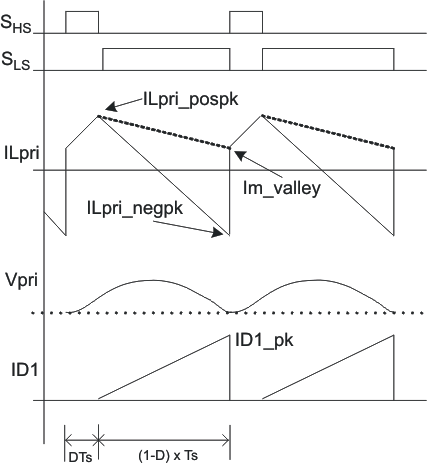 Figure 21. Simplified Voltage and Current Waveforms